Can someone explain the differences? Wii U's architecture is supposedly similar to 360 but it's not limited by low amount of eDRAM, therefore obviously we're not seeing problems with native 720p and even 1080p. But other than that what are the advantages of each type? What would happen if say Xbone had eDRAM and not eSRAM?
-
Hey, guest user. Hope you're enjoying NeoGAF! Have you considered registering for an account? Come join us and add your take to the daily discourse.
You are using an out of date browser. It may not display this or other websites correctly.
You should upgrade or use an alternative browser.
You should upgrade or use an alternative browser.
Wii U's eDRAM vs Xbone's eSRAM. Both have 32 mb. Which one's better?
- Thread starter ShamePain
- Start date
Wii U has 38MB of edram, 3MB on the CPU, 35MB on the GPU, 3MB of which are legacy MB from the gamecube's original GPU (2MB of z-buffer and 1MB of texture cache.)
Xbone's esram is 32MB, but it does have 4MB of L2 cache on the CPU (similar to Wii U's 3MB on the CPU) giving it 36MB of embedded ram.
These serve identical functions, I wouldn't consider them to be advantages over the other, but Wii U's extra 3MB on the GPU should help with some smaller effects, such as fur. Honestly though it must feel like some sort of super power on the Wii U, giving it an unbalanced edge considering it's much lower graphical performance, so I'd give it to Wii U just based on that.
Wii U has 38MB of edram, 3MB on the CPU, 35MB on the GPU, 3MB of which are legacy MB from the gamecube's original GPU (2MB of z-buffer and 1MB of texture cache.)
Xbone's esram is 32MB, but it does have 4MB of L2 cache on the CPU (similar to Wii U's 3MB on the CPU) giving it 36MB of embedded ram.
These serve identical functions, I wouldn't consider them to be advantages over the other, but Wii U's extra 3MB on the GPU should help with some smaller effects, such as fur. Honestly though it must feel like some sort of super power on the Wii U, giving it an unbalanced edge considering it's much lower graphical performance, so I'd give it to Wii U just based on that.
Wouldn't Wii U still be held back by laughable RAM bandwidth? It's got 2 gigs of DDR3 but at like 12 Gb/sec max.
cheezcake
Member
'e' just stands for embedded. SRAM is much faster and also more power efficient than DRAM, it also requires more transistors which makes it more expensive and increases the die area.
In terms of the technical difference, SRAM stands for static random access memory, DRAM stands for dynamic random access memory. They hold memory states in completely different ways. SRAM uses a flip-flop, static comes from the fact that as long as main power stays on the flip flop memory state won't change unless it is explicitly written to.
DRAM uses a transistor-capacitor arrangement, the issue here is capacitors discharge in this configuration so they have to be periodically 'refreshed' to make sure memory values don't change. That's where 'dynamic' comes from and also why it's much slower than SRAM, the refresh operation takes up a large chunk of time.
As above DRAM is MUCH slower than SRAM.
In terms of the technical difference, SRAM stands for static random access memory, DRAM stands for dynamic random access memory. They hold memory states in completely different ways. SRAM uses a flip-flop, static comes from the fact that as long as main power stays on the flip flop memory state won't change unless it is explicitly written to.
DRAM uses a transistor-capacitor arrangement, the issue here is capacitors discharge in this configuration so they have to be periodically 'refreshed' to make sure memory values don't change. That's where 'dynamic' comes from and also why it's much slower than SRAM, the refresh operation takes up a large chunk of time.
Wii U has 38MB of edram, 3MB on the CPU, 35MB on the GPU, 3MB of which are legacy MB from the gamecube's original GPU (2MB of z-buffer and 1MB of texture cache.)
Xbone's esram is 32MB, but it does have 4MB of L2 cache on the CPU (similar to Wii U's 3MB on the CPU) giving it 36MB of embedded ram.
These serve identical functions, I wouldn't consider them to be advantages over the other, but Wii U's extra 3MB on the GPU should help with some smaller effects, such as fur. Honestly though it must feel like some sort of super power on the Wii U, giving it an unbalanced edge considering it's much lower graphical performance, so I'd give it to Wii U just based on that.
As above DRAM is MUCH slower than SRAM.
PumpkinSpice
Banned
SRAM is better than DRAM in nearly all cases. It's faster, much faster, but is very expensive.
'e' just stands for embedded. SRAM is much faster and also more power efficient than DRAM, it also requires more transistors which makes it more expensive and increases the die area.
In terms of the technical difference, SRAM stands for static random access memory, DRAM stands for dynamic random access memory. They hold memory states in completely different ways. SRAM uses a flip-flop, static comes from the fact that as long as main power stays on the flip flop memory state won't change unless it is explicitly written to.
DRAM uses a transistor-capacitor arrangement, the issue here is capacitors discharge in this configuration so they have to be periodically 'refreshed' to make sure memory values don't change. That's where 'dynamic' comes from and also why it's much slower than SRAM, the refresh operation takes up a large chunk of time.
I see now. I was wondering why MS didn't go for eDRAM for Xbone like they did with 360, wasn't it a separate chip next to GPU? Might have freed some die space for more ROPs and what not. But I guess this would be a less effective solution than we have now.
cheezcake
Member
I see now. I was wondering why MS didn't go for eDRAM for Xbone like they did with 360, wasn't it a separate chip next to GPU? Might have freed some die space for more ROPs and what not. But I guess this would be a less effective solution than we have now.
They pretty much had to go for eSRAM, eDRAM would've just murdered them in the BW department. eSRAM gives you something like 110 GB/s min to 204 GB/s peak bandwidth to the GPU. The 360 eDRAM had somewhere along the lines of 30GB/s bandwidth to GPU if I recall correctly. Huge difference.
so basically not comparable...?
Of course it is. It's a memory solution and there are quite a few things that can be compared:
- bandwidth
- latency
- "organization"
- how it is connected to other parts in a system
- how much space it uses
- how much it costs
- is the access "full-duplex"?
...
Brad Grenz
Member
SRAM is better than DRAM in nearly all cases. It's faster, much faster, but is very expensive.
That is not a given. It depends on the configuration used. Compared to the SRAM cache usually seen in GPUs and CPUs, the 32MB in the Xbox One is much, much slower. It is also slower then you might typically expect embedded DRAM to be. In fact it's quite a bit slower than the eDRAM used in the 360.
I don't know that we have bandwidth figures for the WiiU's eDRAM but it could very well have more bandwidth than the Xbox One. It also has a GPU something like 1/8th as powerful. The ratio of size and bandwidth to FLOPs in the Xbox One is actually pretty bad for an embedded memory design.
cheezcake
Member
That is not a given. It depends on the configuration used. Compared to the SRAM cache usually seen in GPUs and CPUs, the 32MB in the Xbox One is much, much slower. It is also slower then you might typically expect embedded DRAM to be. In fact it's quite a bit slower than the eDRAM used in the 360.
I don't know that we have bandwidth figures for the Wii's eDRAM but it could very well have more bandwidth than the Xbox One. It also has a GPU something like 1/8th as powerful. The ratio of size and bandwidth to FLOPs in the Xbox One is actually pretty bad for an embedded memory design.
Wut.
Tal Shiar Agent
Member
Why did Microsoft even include eSRAM at all in the Xbox One. What tangible benefits does it bring and what function does it serve?
Fourth Storm
Member
I see now. I was wondering why MS didn't go for eDRAM for Xbone like they did with 360, wasn't it a separate chip next to GPU? Might have freed some die space for more ROPs and what not. But I guess this would be a less effective solution than we have now.
Having everything on one chip, as in PS4/Xbone, simplifies the design and reduces cost/cooling requirements. The likely reason MS did not spring for eDRAM, however, is that it is proprietary tech and expensive to implement. Only a few companies do it and it wasn't available to MS at 28nm, which their processor is built on.
I have read that the CPU does not have access to the eSRAM on Xbone, whereas on Wii U, the eDRAM can be used as scratchpad memory by the CPU. It is true that SRAM usually has a very low latency, but Wii U's eDRAM is also low latency (although I am not sure how they compare).
The big difference between the two is bandwidth. MS says their eSRAM can do what ~109 GB/s - perhaps twice that if conditions are right? Wii U's eDRAM is ~32 GB/s. It's good enough to do what it's asked to do (buffer a 720p frame and prevent screen tearing), though, whereas Xbone's eSRAM seems to be a bottleneck.
That is not a given. It depends on the configuration used. Compared to the SRAM cache usually seen in GPUs and CPUs, the 32MB in the Xbox One is much, much slower. It is also slower then you might typically expect embedded DRAM to be. In fact it's quite a bit slower than the eDRAM used in the 360.
The esram in Xbone is slower than the edram used in 360? In terms of wait-states for CPU? Or bandwidth (while this is nothing we should give a name in context of "speed")? I don't think either one is "slower"... But I guess you want to augment your post with actual numbers.
Brad Grenz
Member
Wut.
The on chip bandwidth of the 360's 10MB EDRAM is 256GB/s. The ESRAM in the has a typical bandwidth of only 109GB/s with some potential for more than that in ideal read/write operations.
cheezcake
Member
The on chip bandwidth of the 360's 10MB EDRAM is 256GB/s. The ESRAM in the has a typical bandwidth of only 109GB/s with some potential for more than that in ideal read/write operations.
You're mistaking the eDRAMs internal logic to internal memory bandwidth with the eDRAM-GPU memory bus bandwidth. The 256GB/s measurement is how fast eDRAM can basically communicates with itself, not how fast the GPU communicates with it.
The on chip bandwidth of the 360's 10MB EDRAM is 256GB/s. The ESRAM in the has a typical bandwidth of only 109GB/s with some potential for more than that in ideal read/write operations.
Isn't the 360 256Gb?
'e' just stands for embedded. SRAM is much faster and also more power efficient than DRAM, it also requires more transistors which makes it more expensive and increases the die area.
In terms of the technical difference, SRAM stands for static random access memory, DRAM stands for dynamic random access memory. They hold memory states in completely different ways. SRAM uses a flip-flop, static comes from the fact that as long as main power stays on the flip flop memory state won't change unless it is explicitly written to.
DRAM uses a transistor-capacitor arrangement, the issue here is capacitors discharge in this configuration so they have to be periodically 'refreshed' to make sure memory values don't change. That's where 'dynamic' comes from and also why it's much slower than SRAM, the refresh operation takes up a large chunk of time.
As above DRAM is MUCH slower than SRAM.
The legacy embedded memory is sram in the Wii U's GPU, since operations you'd do at this speed is very limited, and for smaller effects, 3MB is enough to handle those situations. This larger 32MB buffer is usually used for frame buffer, which only needs to be fast enough to give 60fps @ a given resolution, edram is more than fast enough for this, and at 720p there is plenty of room left over for effects as well.
My point with Wii U's cache being better, is that it is a luxury, considering the much lower performance of the Wii U's GPU, it is proportionally more of an edge for Wii U.
xbone
wiiu


I am not an xbone developer so I'm not sure why those chunks are split up, but if I remember right, Xbox1's GPU, CPU and Memory are all split in 2 modules, seems very curious why they did this with memory.
Why did Microsoft even include eSRAM at all in the Xbox One. What tangible benefits does it bring and what function does it serve?
MS knew quite early that they wanted to have 8 GB RAM in the Xbone. I guess by that time GDDR5 just was no option for them to use so they had to find another solution and went a similar approach like they did with 360.
The purpose is that devs should adjust their engines to make the best use of the esram which needs modification for dev-engines. For example, deferred rendering is bad as it requires a lot of space in memory which Xbone doesn't have (see Fox engine and why all Xbone games with Fox engine are 720p). Forward renderers are not that heavy so they better fit in the esram.
Here is a link for you: http://bit.ly/1EQeW8D
The on chip bandwidth of the 360's 10MB EDRAM is 256GB/s. The ESRAM in the has a typical bandwidth of only 109GB/s with some potential for more than that in ideal read/write operations.
Ok, it's a misunderstanding on your side.
Fourth Storm
Member
Isn't the 360 256Gb?
Nope, it's gigabytes, but that bandwidth is only to the ROPs. 360's GPU is a funky design where the ROPs are off-chip w/ the eDRAM. Was meant for easier AA. From the ROPs/eDRAM to the rest of the GPU is ~30GB/s.
Projectjustice
Banned
Using external memory, the GPU would be limited to a 32- or 64-bit interface. The NEC Electronics eDRAM expands the on-chip memory interface past 1000 bits in width to support the GPU’s 256-Gbytes/second bandwidth between the graphics pipelines and memory.”
It's been speculated that taking the information above into consideration, the Wii U's total bandwidth of gigabytes per second, including the possible 1024 bits per macro and GPU – which, according to TechPowerUp clocks in at 550mhz – would come out to around 563.2GB per second. Keep in mind that the Xbox One runs about 170GB per second of bandwidth between the DDR3 and eSRAM, as outlined by Xbit Labs.
http://www.cinemablend.com/games/Wii-U-Memory-Bandwidth-GPU-More-Powerful-Than-We-Thought-62437.html
Dont know how accurate this is but I found it interesting nonetheless.
OnionPowder
Member
Why did Microsoft even include eSRAM at all in the Xbox One. What tangible benefits does it bring and what function does it serve?
It's the only way to make DDR3 work IIRC. GDDR5 was a gamble because as of like January 2013 4GB was the max they could do.
Enlightening as always.Having everything on one chip, as in PS4/Xbone, simplifies the design and reduces cost/cooling requirements. The likely reason MS did not spring for eDRAM, however, is that it is proprietary tech and expensive to implement. Only a few companies do it and it wasn't available to MS at 28nm, which their processor is built on.
I have read that the CPU does not have access to the eSRAM on Xbone, whereas on Wii U, the eDRAM can be used as scratchpad memory by the CPU. It is true that SRAM usually has a very low latency, but Wii U's eDRAM is also low latency (although I am not sure how they compare).
The big difference between the two is bandwidth. MS says their eSRAM can do what ~109 GB/s - perhaps twice that if conditions are right? Wii U's eDRAM is ~32 GB/s. It's good enough to do what it's asked to do (buffer a 720p frame and prevent screen tearing), though, whereas Xbone's eSRAM seems to be a bottleneck.
Brad Grenz
Member
You're mistaking the eDRAMs internal logic to internal memory bandwidth with the eDRAM-GPU memory bus bandwidth. The 256GB/s measurement is how fast eSRAM can basically communicates with itself, not how fast the GPU communicates with it.
I'm not confusing anything. The EDRAM in the 360 is not simply off chip memory on a daughter die. They also moved the most bandwidth heavy consumers of a GPU the ROPs, to the same die. In any case the speed of the EDRAM is the speed of the EDRAM and citing the speed of a chip to chip interface instead is misleading.
cheezcake
Member
http://www.cinemablend.com/games/Wii-U-Memory-Bandwidth-GPU-More-Powerful-Than-We-Thought-62437.html
Dont know how accurate this is but I found it interesting nonetheless.
It's literally 100% bull plop. They take the eDRAM internal logic-memory BW number and compare it to the eSRAM die-GPU BW, apples and oranges. They then seemingly apply Moore's Law to speed...Moore's law is about increasing transistor density for cost and has no bearing on bandwidth.
Nope, it's gigabytes, but that bandwidth is only to the ROPs. 360's GPU is a funky design where the ROPs are off-chip w/ the eDRAM. Was meant for easier AA. From the ROPs/eDRAM to the rest of the GPU is ~30GB/s.
Ahh I see. Nevermind then
Barkley's Justice
Member
This question keeps me up at night.
I'm not confusing anything. The EDRAM in the 360 is not simply off chip memory on a daughter die. They also moved the most bandwidth heavy consumers of a GPU the ROPs, to the same die. In any case the speed of the EDRAM is the speed of the EDRAM and citing the speed of a chip to chip interface instead is misleading.
How fast can the GPU read/write from/to EDRAM?
cheezcake
Member
I'm not confusing anything. The EDRAM in the 360 is not simply off chip memory on a daughter die. They also moved the most bandwidth heavy consumers of a GPU the ROPs, to the same die. In any case the speed of the EDRAM is the speed of the EDRAM and citing the speed of a chip to chip interface instead is misleading.
Dude just look at the diagram. How is the GPU going to feed the ROPs without first being BW limited by the actual eDRAM-GPU bus BW which is 32 GB/s. Again you're comparing apples and oranges, the eSRAM BW figure everyone hears is the bandwidth on the GPU->eSRAM bus. The corresponding GPU->eDRAM bus bandwidth on the 360 is 32GB/s. By comparing the 256GB/s number with the Xbones eSRAM number you're comparing entirely different things.
Having everything on one chip, as in PS4/Xbone, simplifies the design and reduces cost/cooling requirements. The likely reason MS did not spring for eDRAM, however, is that it is proprietary tech and expensive to implement. Only a few companies do it and it wasn't available to MS at 28nm, which their processor is built on.
SRAM is more expensive than DRAM byte for byte in every case, it also requires more die space and is hence more difficult to implement.
Brad Grenz
Member
How fast can the GPU read/write from/to EDRAM?
256GB/s.
Maybe you guys are confused, but a delineation between internal logic bandwidth and an off chip gpu connection is actually unorthodox. In a single chip design like the WiiU and Xbox One GPUs have there is no reason to introduce any limit on the EDRAM's maximum potential bandwidth. In that case the "internal logic" bandwidth and the bandwidth to the GPU are one in the same. The "logic" in question is GPU logic.
cheezcake
Member
The legacy embedded memory is sram in the Wii U's GPU, since operations you'd do at this speed is very limited, and for smaller effects, 3MB is enough to handle those situations. This larger 32MB buffer is usually used for frame buffer, which only needs to be fast enough to give 60fps @ a given resolution, edram is more than fast enough for this, and at 720p there is plenty of room left over for effects as well.
My point with Wii U's cache being better, is that it is a luxury, considering the much lower performance of the Wii U's GPU, it is proportionally more of an edge for Wii U.
xbone
wiiu
I am not an xbone developer so I'm not sure why those chunks are split up, but if I remember right, Xbox1's GPU, CPU and Memory are all split in 2 modules, seems very curious why they did this with memory.
Sorry I'm not getting something, you're saying Wii U's cache is better where is that stemming from? L2 cache on the jaguar will be SRAM also but on the CPU SOC? (I'm not sure about this). But that effectively means X1 cache is better even if it isn't on SOC considering it has 4MB vs 3MB on the Wii U. But if we're debating which system has the better suited memory architecture I will definitely agree with you that Wii U's is more appropriate given the weaker GPU.
256GB/s.
Maybe you guys are confused, but a delineation between internal logic bandwidth and an off chip gpu connection is actually unorthodox. In a single chip design like the WiiU and Xbox One GPUs have there is no reason to introduce any limit on the EDRAM's maximum potential bandwidth. In that case the "internal logic" bandwidth and the bandwidth to the GPU are one in the same. The "logic" in question is GPU logic.
http://en.wikipedia.org/wiki/Xbox_360_technical_specifications#Memory_and_system_bandwidth
The console features 512 MB of GDDR3 RAM clocked at 700 MHz with an effective transmission rate of 1.4 GHz on a 128-bit bus. The memory is shared by the CPU and the GPU via the unified memory architecture. This memory is produced by either Samsung or Qimonda.
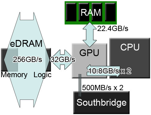
The Xbox 360 has an extensive amount of bandwidth in comparison to its competition;[6] however, this statistic includes the eDRAM logic to memory bandwidth, and not internal CPU bandwidths. The eDRAM internal logic to its internal memory bandwidth is 256 GB/s. The high bandwidth is used primarily for z-buffering, alpha blending, and antialiasing; it saves time and space on the GPU die. Between the eDRAM die and the GPU, data is transferred at 32 GB/s.[7] The memory interface bus has a bandwidth of 22.40 GB/s and the Southbridge a bandwidth of 500 MB/s.
Brad Grenz
Member
What do you think that proves? Nothing in what you quoted contradicts what I've said.
cheezcake
Member
256GB/s.
Maybe you guys are confused, but a delineation between internal logic bandwidth and an off chip gpu connection is actually unorthodox. In a single chip design like the WiiU and Xbox One GPUs have there is no reason to introduce any limit on the EDRAM's maximum potential bandwidth. In that case the "internal logic" bandwidth and the bandwidth to the GPU are one in the same. The "logic" in question is GPU logic.
I see where the confusion is coming from now that I've done a bit of reading. The eDRAM logic refers to obviously the support logic used to manage read/write/refresh cycles but they also built in some extra logic to perform z-testing, alpha blending and some AA purely between the eDRAM logic and memory bank, bypassing the GPU BW limit when performing ONLY these operations. That's the other thing, that's only three classes of operations which you can effectively say the GPU has 256GB/s BW for, everything else is still limited by the 32 GB/s GPU->eDRAM bus. And that everything else is a lot of things.
Very clever design, but nonetheless claiming the GPU->eDRAM BW is always 256GB/s is downright wrong.
Fourth Storm
Member
SRAM is more expensive than DRAM byte for byte in every case, it also requires more die space and is hence more difficult to implement.
This is true, but foundries have SRAM libraries as a basic option for any given process node. This is not the case for DRAM--or at least the manufacturing specifications for DRAM are different than what they use for processors, so integration onto a single die is not a trivial matter. NEC/Renesas, IBM, and Intel take special care when designing a node, applying trench capacitors, insulator, and various other proprietary techniques, so that they are compatible w/ DRAM cells. It's tough to know how much MS spent on the eSRAM interface, DMAs, and etc., but I'd say, on average, adding eDRAM to a design will end up costing you more.
cheezcake
Member
This is true, but foundries have SRAM libraries as a basic option for any given process node. This is not the case for DRAM--or at least the manufacturing specifications for DRAM are different than what they use for processors, so integration onto a single die is not a trivial matter. NEC/Renesas, IBM, and Intel take special care when designing a node, applying trench capacitors, insulator, and various other proprietary techniques, so that they are compatible w/ DRAM cells. It's tough to know how much MS spent on the eSRAM interface, DMAs, and etc., but I'd say, on average, adding eDRAM to a design will end up costing you more.
Ah that's interesting to know, I'm not too knowledgable on the manufacturing supply side of things. Still just an elec eng student so mostly just familiar with the technical theory.
Though that does beg the question is the die space saved when using DRAM worth the extra cost and lower BW?
The on chip bandwidth of the 360's 10MB EDRAM is 256GB/s. The ESRAM in the has a typical bandwidth of only 109GB/s with some potential for more than that in ideal read/write operations.
The 256GB/s figure is tied to 4xMSAA as it's fully uncompressed for the 360 ROPs.
This is true, but foundries have SRAM libraries as a basic option for any given process node. This is not the case for DRAM--or at least the manufacturing specifications for DRAM are different than what they use for processors, so integration onto a single die is not a trivial matter. NEC/Renesas, IBM, and Intel take special care when designing a node, applying trench capacitors, insulator, and various other proprietary techniques, so that they are compatible w/ DRAM cells. It's tough to know how much MS spent on the eSRAM interface, DMAs, and etc., but I'd say, on average, adding eDRAM to a design will end up costing you more.
Possibly. But eDRAM does not need to be on die to be considered eDRAM (I suppose eSRAM doesn't either). This means that it could simply be put on package like most other implementations. I did read that intel did do a lot of work for their eDRAM implementation in Haswell, so it could be the case of the immediate availability of eSRAM at the cost of inflated die sizes, vs researching a working eDRAM solution that would work with the bandwidth requirements and thermal constraints.
Insane Metal
Member
I think there's no such thing as 'which one is better', both are there for different purposes and they do what they're supposed to.
Melchiah
Member
You're mistaking the eDRAMs internal logic to internal memory bandwidth with the eDRAM-GPU memory bus bandwidth. The 256GB/s measurement is how fast eSRAM can basically communicates with itself, not how fast the GPU communicates with it.
That's pretty humorous in retrospect, considering this old article by Major Nelson.
http://majornelson.com/2005/05/20/xbox-360-vs-ps3-part-1-of-4/
The memory system bandwidth in Xbox 360 exceeds the PS3s by five times.

Though that does beg the question is the die space saved when using DRAM worth the extra cost and lower BW?
MS will reap benefits from node size reductions in the case of eSRAM.
However DRAM would allow for much more RAM. according to Intel they determined that the ideal size of the eDRAM cache was between 64MB and 128MB with only 64GB/s of bandwidth on a 512bit bus. I don't know if any other manufacturer could provide more bandwidth, but then again once you leave the AMD design and start mixing different foundries the price will start to add up.
So I'd probably revise my statement before and say that MS pretty much was locked into eSRAM from a cost standpoint.
DRAM uses a transistor-capacitor arrangement, the issue here is capacitors discharge in this configuration so they have to be periodically 'refreshed' to make sure memory values don't change. That's where 'dynamic' comes from and also why it's much slower than SRAM, the refresh operation takes up a large chunk of time.
The bolded part is not correct. Although DRAM refresh takes some time, it needs to be done rather infrequently. A typical requirement is once every 64 ms, i.e. less than 16 times per second. The refresh can be done in parallel with a cycle time similar to a normal access, and even without perfect parallelization, 16 refresh events per second is very modest compared to the hundreds of millions of normal accesses during that second.
The main reason why DRAM is slower than SRAM lies rather in the actual read and write operations being more delicate and time consuming.
The main reason why DRAM is slower than SRAM lies rather in the actual read and write operations being more delicate and time consuming.
The fact that it is capacitor based should clue one in as to why it is slower than sram. As stated above reading and writing require multiple stages in order to actually access the data. The large bit line lengths also impose a certain amount of propagation delay when reading and writing.
Fourth Storm
Member
Possibly. But eDRAM does not need to be on die to be considered eDRAM (I suppose eSRAM doesn't either). This means that it could simply be put on package like most other implementations. I did read that intel did do a lot of work for their eDRAM implementation in Haswell, so it could be the case of the immediate availability of eSRAM at the cost of inflated die sizes, vs researching a working eDRAM solution that would work with the bandwidth requirements and thermal constraints.
It should be on-die to qualify. I'd say the 360's barely qualifies only because it has that logic on the die w/ the eDRAM. And then with eSRAM, that's more an MS term to describe the function in somewhat familiar terms to console owners, I think. Most SRAM is embedded in a larger processor.
Yeah, the eSRAM was immediately available and could be manufactured by TSMC, Global Foundries, or whoever. The only people that currently design/produce eDRAM nowadays are IBM and Intel, both of whom would presumably only allow their tech to be used alongside one of their own processors. Then, there is NEC/Renesas, whose eDRAM is found in Wii U. But they are stuck at the 45nm/40nm process node.
Technically, they could have gone w/ NEC/Renesas again, and used an MCM design like 360/Wii U, but then that issue creeps up again that they would be stuck with one supplier.
ninjablade
Banned
Having everything on one chip, as in PS4/Xbone, simplifies the design and reduces cost/cooling requirements. The likely reason MS did not spring for eDRAM, however, is that it is proprietary tech and expensive to implement. Only a few companies do it and it wasn't available to MS at 28nm, which their processor is built on.
I have read that the CPU does not have access to the eSRAM on Xbone, whereas on Wii U, the eDRAM can be used as scratchpad memory by the CPU. It is true that SRAM usually has a very low latency, but Wii U's eDRAM is also low latency (although I am not sure how they compare).
The big difference between the two is bandwidth. MS says their eSRAM can do what ~109 GB/s - perhaps twice that if conditions are right? Wii U's eDRAM is ~32 GB/s. It's good enough to do what it's asked to do (buffer a 720p frame and prevent screen tearing), though, whereas Xbone's eSRAM seems to be a bottleneck.
always love reading your very informative posts with out bias, thanks.