• Hey, guest user. Hope you're enjoying NeoGAF! Have you considered registering for an account? Come join us and add your take to the daily discourse.

Architectural details on Nvidia's Maxwell - Efficiency to the power of WATT

artist

Banned
Videocardz seem to have landed some juicy details on the upcoming Maxwell.

First up the Cuda core count;
Full GM107 has 5 SMs with 128 CUDAs each, which gives 640 in total. This means that GTX 750 Ti has 640 CUDAs (5 SMX) and GTX 750 has 512 (4 SMX).

TDP;
GM107 has a TDP of 60W

The GM107 will not even utilize the full power delivered by PCI-E connector (75W). While operating at default frequencies it won’t need any additional power source. Although manufacturers will still add the power connector, for the sake of stability or increasing the overclocking headroom.

Maxwell is said to deliver twice the performance per watt of Kepler.

Maxwell Generations;
There are two generations of Maxwell GPUs
It has been revealed by newest CUDA driver that NVIDIA will make two generations of Maxwell GPUs:

28nm: GM108, GM107
20nm: GM206, GM204, GM200

SM Details
Meet the SMM (Maxwell Streaming Multiprocessor)
Maxwell introduces new architecture, which is not exactly revolutionary, but definitely new. The streaming multiprocessor known from Fermi and Kepler received the biggest change. Those who thought that Maxwell architecture will introduce more CUDAs in each multiprocessor will be disappointed. In fact, each SMM is split into four blocks of operating units. Each of those blocks holds 32 CUDA cores, so the full SMM has 4 × 32 = 128 CUDAs. You can find here references to both Fermi and Kepler.
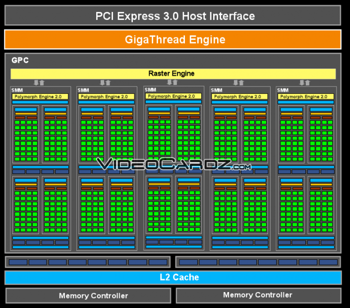
maxwell-gm107-706x620eokir.png


This is the first ever diagram of Maxwell GPU. There is one Graphics Processing Cluster. Full GM107 has 5 SMMs with 640 cores in total. Each SMM has 8 TMUs, so the total count is 40. The GPU has 16 ROPs and two memory controllers (both 64b).

What is new in Maxwell
Okay, so the SM has been redesigned, the layout has changed, but what exactly makes the Maxwell better? Well here’s the list:

Larger L2 cache.
This is the main difference between Kepler and Maxwell. Larger L2 cache will limit the queries to the GPU. GM107 L2 cache has 2MB. GK107′s cache has 256KB.
Workload balancing and complier-based scheduling has been improved.
The number of instructions per clock cycle has been increased.
SM has been redesigned into four processing blocks (as explained above).
Maxwell introduces even faster H.264 encoding and decoding with improved NVENC (which is used, for instance, in ShadowPlay).
New GC5 power state (low sleep state).

Efficiency;
GM107 has a die size of 148mm2
As opposed to previous leaks, the die size of GM107 is even smaller, not 156 but 148mm2. Compared to GK107 the density of CUDAs per mm2 has increased roughly by 30%. The density of transistors increased by 15%. Remember, this is all on the same fabrication process.
http://videocardz.com/49557/exclusive-nvidia-maxwell-gm107-architecture-unveiled

I'm guessing GTX860Ti = 1920/1792 cores Q4 '14. GTX880 = 2560 cores, Q1 '15. Titan successor = 3840 cores, Q2 '15.
 

dr_rus

Member
I'm guessing GTX860Ti = 1920/1792 cores Q4 '14. GTX880 = 2560 cores, Q1 '15. Titan successor = 3840 cores, Q2 '15.
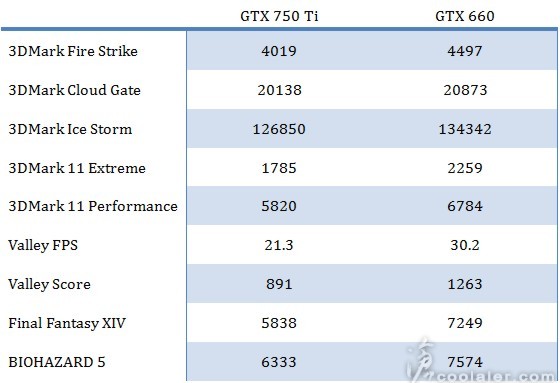
GM20x parts are very likely to have a different GPC/SM/SIMD balance.

How badly is this going to blow away my 780?
GTX750/Ti parts are coming to current GTX650/Ti price/performance brackets.
Your 780 is fine till 20nm GPUs hit the market.
 

mrklaw

MrArseFace
If 880 is Q1 2015 I may kill myself. My upgrade plans were based on the assumption of a Q2 2014 release, or Q3 at the latest.

almost guaranteed not to be Q2 (we are pretty much there now and we've seen nothing but peeks at the lower end cards), and I think Q3 is looking dodgy too.
 

M3d10n

Member
Maybe it's supposed to compete against the HD 7850 (since the 660 is more expensive and the 650 is slower).
 

AmyS

Member
I'll be fine with the 28nm Kepler 780 Ti for a long time.

Won't consider a Maxwell part until it is a.) on 20nm b) a full high-end Maxwell GPU.

So probably not until 2015.


There's plenty of time to evaluate the Maxwell architecture to make a choice about when and where to jump aboard. Maxwell GPUs are gonna to be around for years.

Next Nvidia GPU architecture after Maxwell, Volta, with stacked DRAM / memory and, according to Jen-Hsun: 1 TeraByte per sec memory bandwidth because of the stacked memory. Volta won't arrive until 2016 at the soonest, and we all know how things slip on NV's roadmaps.

http://www.anandtech.com/show/6846/nvidia-updates-gpu-roadmap-announces-volta-family-for-beyond-2014

zB3njKW.jpg


hqdSHuh.jpg


In any case, Volta’s marque feature will be stacked DRAM, which sees DRAM placed very close to the GPU by placing it on the same package, and connected to the GPU using through-silicon vias (TSVs). Having high bandwidth, on-package RAM is not new technology, but it is still relatively exotic. In the GPU world the most notable shipping product using it would be the PS Vita, which has 128MB of RAM in a wide-IO (but not TSV) manner. Meanwhile NVIDIA competitor Intel will be using a form of embedded DRAM for their highest-performance GT3e iGPU for their forthcoming Haswell generation CPUs.

The advantage of stacked DRAM for a GPU is that its locality brings with it both bandwidth and latency benefits. In terms of bandwidth the memory bus can be both faster and wider than an external memory bus, depending on how it’s configured. Specifically the close location of the DRAM to the GPU makes it practical to run a wide bus, while the short traces can allow for higher clockspeeds. Meanwhile the proximity of the two devices means that latency should be a bit lower – a lot of the latency is in the RAM fetching the required cells, but at the clockspeeds GDDR5 already operates at the memory buses on a GPU are relatively long, so there are some savings to be gained.

NVIDIA is targeting a 1TB/sec bandwidth rate for Volta, which to put things in perspective is over 3x what GeForce GTX Titan currently achieves with its 384bit, 6Gbps/pin memory bus (288GB/sec). This would imply that Volta is shooting for something along the lines of a 1024bit bus operating at 8Gbps/pin, or possibly an even larger 2048bit bus operating at 4Gbps/pin. Volta s still years off, but this at least gives us an idea of what NVIDIA needs to achieve to hit their 1TB/sec target.

What will be interesting to see is how NVIDIA handles the capacity issues brought on by on-chip RAM. It’s no secret that DRAM is rather big, and especially so for GDDR. Moving all of that RAM on-chip seems unlikely, especially when consumer video cards are already pushing 6GB (Titan). For high-end GPUs this may mean NVIDIA is looking at a split RAM configuration, with the on-chip RAM acting as a cache or small pool of shared memory, while a much larger pool of slower memory is attached via an external bus.

At this point Volta does not have a date attached to it, which is unlike Maxwell which originally had a 2013 date attached to it when first named. That date of course slipped to 2014, and while it’s never been made clear why, the fact that Kepler slipped from 2011 to 2012 is a reminder that NVIDIA is still tied to TSMC’s production schedule due to their preference to launch new architectures on new nodes. Volta in turn will have some desired node attached to its development, but we don’t know what at this time.

With TSMC shaking up its schedule in an attempt to catch up to Intel on both nodes and technology, the lack of a date ultimately is not surprising since it’s difficult at best to predict when the appropriate node will be ready 3 years out.


Nvidia CEO Jen-Hsun on Volta at GTC 2013
http://www.youtube.com/watch?v=BYJ1-XQzHx4

Yeah, Maxwell is gonna be around a long time. I'm taking a wait 'n see approach.
 

tipoo

Banned
I want to know what that ARM core in the higher end Maxwell parts will do. It's just a "command processor" rather than full ARM core in the lower end ones.
 

solarus

Member
Hmmm to maxwell or ride it out until volta. I was thinking that the next time i get a beefy gpu would be when the consumer version of occulus rift comes out (or the second consumer version).
 

Jtrizzy

Member
I'm hoping they have something I want by July. I want that 1440p 120hz 3d gsync asus, but I'll need something beefy to power it.
 
One number jumped out - 16 rops. Isn't that one of the things holding back the xbone allegedly? Or is that an apples to oranges comparison?
 

Tablo

Member
I was hoping for a h.265 encoder/decoder. That would be sweet. Is that standard just not mature enough yet to add hardware acceleration?
 

elyetis

Member
If 880 is Q1 2015 I may kill myself. My upgrade plans were based on the assumption of a Q2 2014 release, or Q3 at the latest.
Same here, same here... my 2x570 still work pretty well on recent games but the need to upgrade is getting stronger and stronger ( and will be even more once star citizen dog fight module get released, let alone if the oculust rift keep it's 2014 release date ).
 
Top Bottom