Videocardz seem to have landed some juicy details on the upcoming Maxwell.
First up the Cuda core count;
TDP;
Maxwell Generations;
SM Details
Efficiency;
I'm guessing GTX860Ti = 1920/1792 cores Q4 '14. GTX880 = 2560 cores, Q1 '15. Titan successor = 3840 cores, Q2 '15.
First up the Cuda core count;
Full GM107 has 5 SMs with 128 CUDAs each, which gives 640 in total. This means that GTX 750 Ti has 640 CUDAs (5 SMX) and GTX 750 has 512 (4 SMX).
TDP;
GM107 has a TDP of 60W
The GM107 will not even utilize the full power delivered by PCI-E connector (75W). While operating at default frequencies it wont need any additional power source. Although manufacturers will still add the power connector, for the sake of stability or increasing the overclocking headroom.
Maxwell is said to deliver twice the performance per watt of Kepler.
Maxwell Generations;
There are two generations of Maxwell GPUs
It has been revealed by newest CUDA driver that NVIDIA will make two generations of Maxwell GPUs:
28nm: GM108, GM107
20nm: GM206, GM204, GM200
SM Details
Meet the SMM (Maxwell Streaming Multiprocessor)
Maxwell introduces new architecture, which is not exactly revolutionary, but definitely new. The streaming multiprocessor known from Fermi and Kepler received the biggest change. Those who thought that Maxwell architecture will introduce more CUDAs in each multiprocessor will be disappointed. In fact, each SMM is split into four blocks of operating units. Each of those blocks holds 32 CUDA cores, so the full SMM has 4 × 32 = 128 CUDAs. You can find here references to both Fermi and Kepler.
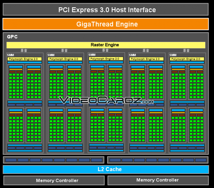
This is the first ever diagram of Maxwell GPU. There is one Graphics Processing Cluster. Full GM107 has 5 SMMs with 640 cores in total. Each SMM has 8 TMUs, so the total count is 40. The GPU has 16 ROPs and two memory controllers (both 64b).
What is new in Maxwell
Okay, so the SM has been redesigned, the layout has changed, but what exactly makes the Maxwell better? Well heres the list:
Larger L2 cache.
This is the main difference between Kepler and Maxwell. Larger L2 cache will limit the queries to the GPU. GM107 L2 cache has 2MB. GK107′s cache has 256KB.
Workload balancing and complier-based scheduling has been improved.
The number of instructions per clock cycle has been increased.
SM has been redesigned into four processing blocks (as explained above).
Maxwell introduces even faster H.264 encoding and decoding with improved NVENC (which is used, for instance, in ShadowPlay).
New GC5 power state (low sleep state).
Efficiency;
http://videocardz.com/49557/exclusive-nvidia-maxwell-gm107-architecture-unveiledGM107 has a die size of 148mm2
As opposed to previous leaks, the die size of GM107 is even smaller, not 156 but 148mm2. Compared to GK107 the density of CUDAs per mm2 has increased roughly by 30%. The density of transistors increased by 15%. Remember, this is all on the same fabrication process.
I'm guessing GTX860Ti = 1920/1792 cores Q4 '14. GTX880 = 2560 cores, Q1 '15. Titan successor = 3840 cores, Q2 '15.