InsaneZero
Member
Surprised that the DF thread got locked.
I don't remember this (but it's pretty much a given), although i said a "branded next gen game" will come to Wii U.
There's a possibility to lighten the die shot to better scrutinize all the brown part besides eDram ? Plox plox plox !

The DF article thread got locked, anyone know why?
The DF article thread got locked, anyone know why?
Because the article is shit, or gaffers went a bit too excited. Maybe both.The DF article thread got locked, anyone know why?
Thanks to show that nothing is solved yet Thraktor !The Digital Foundry Hypothesis
SPUs: 8 blocks (N1-N8)
TMUs: 4 blocks (J1-J4)
ROPS: 2 blocks ? (no proposed location)
ARM: 1 block (no proposed location)
DSP: 1 block (no proposed location)
Video encode/decode: 1 block (no proposed location)
Total blocks explained: 17 (12 with locations)
Total blocks unexplained: 23
The DF article thread got locked, anyone know why?
Because it is a most basic example of GAF->internet->GAF, and the OP of that thread was framed in a very poor way that encouraged drive-by trolling.
We already have this thread which was the source for the Digital Foundry article to begin with.
Because it is a most basic example of GAF->internet->GAF, and the OP of that thread was framed in a very poor way that encouraged drive-by trolling.
We already have this thread which was the source for the Digital Foundry article to begin with.
They didn't even link to the thread here...
Edit: Reposted for the new page:

The Digital Foundry Hypothesis
SPUs: 8 blocks (N1-N8)
TMUs: 4 blocks (J1-J4)
ROPS: 2 blocks ? (no proposed location)
ARM: 1 block (no proposed location)
DSP: 1 block (no proposed location)
Video encode/decode: 1 block (no proposed location)
Total blocks explained: 17 (12 with locations)
Total blocks unexplained: 23
Awesome work
Do you have any understanding why the repeating logic sections differ slightly from each other? Is this common or also unusual?
According to your diagram, there are an additional 3 repeating sections. 1 of them must be the ROPS. Any clue what the other two could be?
Also, DF did mention the command processor.
I'm fascinated by this whole thing. The impression I get is that most of the people with a stick in their ass about the Wii U don't own it and have no plans to. Odd, then, that they're so upset by it.
Even more fascinating are the folks who just, no matter what, really have venom for Nintendo fans. Not for any good reason, mind you...they're just affected deeply by someone who would DARE to have different interests than themselves.
Oh, there are plenty of good reasons to have a distaste for some Nintendo fans. Go read some of the Wii U speculation threads.Even more fascinating are the folks who just, no matter what, really have venom for Nintendo fans. Not for any good reason, mind you...they're just affected deeply by someone who would DARE to have different interests than themselves.
I'm fascinated by this whole thing. The impression I get is that most of the people with a stick in their ass about the Wii U don't own it and have no plans to. Odd, then, that they're so upset by it.
Even more fascinating are the folks who just, no matter what, really have venom for Nintendo fans. Not for any good reason, mind you...they're just affected deeply by someone who would DARE to have different interests than themselves.
The Digital Foundry Hypothesis
SPUs: 8 blocks (N1-N8)
TMUs: 4 blocks (J1-J4)
ROPS: 2 blocks ? (no proposed location)
ARM: 1 block (no proposed location)
DSP: 1 block (no proposed location)
Video encode/decode: 1 block (no proposed location)
Total blocks explained: 17 (12 with locations)
Total blocks unexplained: 23

Someone should do a more in-depth investigation of what's the fraction of "unexplained" die space on a normal AMD GPU (e.g. RV770) compared to this. I think it's not as different as people would expect, particularly considering BC, the ARM core and the DSP.
If no one does it before I'll do it this evening.
I think it's more than that, it just looks like less since its around the periphery. I'll measure it later.Going by the RV770 die shot on the first page, it looks like something in the 10%-20% range. Of course, the ratios may change for a lower-end chip such as this.
I think it's more than that, it just looks like less since its around the periphery. I'll measure it later.
Looking over thing I think we can assume that core parts of the chip are based of the 5550 LE (redwood core). Everything seems to fit, same clock speed, same GFLOPS, 40nm process. Just seems like too simular for it not to be based on that design. Of course there's all the other stuff on the die that we have little clue about.
About the Mem1/Mem2 thing
How exactly does that work?
Is the 32mb edram considered the main RAM? Why else would you name it Mem1?
If so, does Wii U store data it needs into Mem2 and preloads stuff that it needs next into the Mem1, the edram? To make use of its high bandwidth compared to gDDR3?
Is the edram now 140gb/sec or 70gb/sec?
Sorry for all the questions...
Considering Marcan calls that pool "MEM0", that might actually be what it is in native mode. That would suggest that the pool is freely accessible.Great work on the diagram, Thraktor!
Of course, now marcan steps up to reveal more info! What use is a 2 MB eFB besides Wii BC? It's only enough for an SD image. Oh yeah...
I'm fascinated by this whole thing. The impression I get is that most of the people with a stick in their ass about the Wii U don't own it and have no plans to. Odd, then, that they're so upset by it.
Even more fascinating are the folks who just, no matter what, really have venom for Nintendo fans. Not for any good reason, mind you...they're just affected deeply by someone who would DARE to have different interests than themselves.
About the Mem1/Mem2 thing
How exactly does that work?
Is the 32mb edram considered the main RAM? Why else would you name it Mem1?
If so, does Wii U store data it needs into Mem2 and preloads stuff that it needs next into the Mem1, the edram? To make use of its high bandwidth compared to gDDR3?
Is the edram now 140gb/sec or 70gb/sec?
Sorry for all the questions...
And the GDDR3 would act like the DVD.
Is B Florida?
Considering Marcan calls that pool "MEM0", that might actually be what it is in native mode. That would suggest that the pool is freely accessible.
Is B Florida?
Nope, it's eDRAM's mullet.
I'd say its a safe bet the larger 1GB pool is still the "main" memory in the sense that it stores more, like how in your computer your processor has an L1, L2, maybe L3 cache but still has larger main memory. The eDRAM is probably used for high bandwidth GPU operations, a framebuffer, maybe a scratch space between GPU and CPU, but not most of the game memory since that obviously needs more than 32MB.
I think the eDRAM is the main memory in the sense that it holds the most important things (framebuffer, etc.). Less important data (eg textures) go into the much larger secondary DDR3 memory pool.
There's that "V" block that some people have mentioned to be similar to others in the newest AMD GPUs. Maybe the tesselation unit?
Is B Florida?
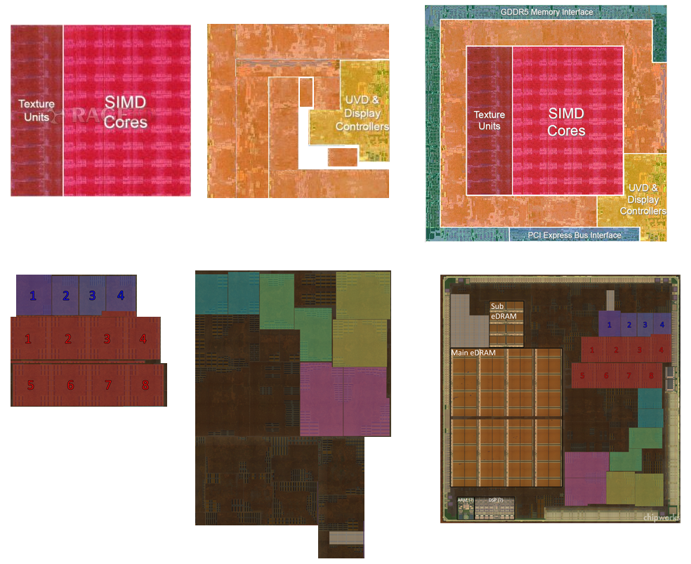
1) The non-TMU/non-SIMD/non-IO parts of RV770 are about as big as the SIMD/TMU parts. And that GPU has a lot of SIMD/TMUs.
2) The non-TMU/non-SIMD/non-IO parts of Wii U's GPU, using the original assumptions, are about 2.4 times as big as the SIMD/TMU parts.
3) The latter includes at least 1 ARM CPU, a DSP, logic for managing and interfacing with 2 separate pools of eDRAM, and maybe some BC components.
My conclusion: If there is some special GPU sauce, it's not all that significant.
Not completely, no. But I do think if his theory were true there would be a bit of a lack of space for "other stuff" that seems to be necessary for a GPU, as the RV770 relative size of components shows.Do you think this disqualifies Thraktor's theory about assymetric shaders?
Usually legendary.While it is disappointing to hear this thing is anemic on the power side but as long as the games come rolling along it really doesn't matter in the end game. Nintendo is legendary because of their first party support so they will be fine.
Someone should do a more in-depth investigation of what's the fraction of "unexplained" die space on a normal AMD GPU (e.g. RV770) compared to this. I think it's not as different as people would expect, particularly considering BC, the ARM core and the DSP.
If no one does it before I'll do it this evening.
Going by the RV770 die shot on the first page, it looks like something in the 10%-20% range. Of course, the ratios may change for a lower-end chip such as this.
I think it's more than that, it just looks like less since its around the periphery. I'll measure it later.
If you rearrange the orange parts in your preferred picture editing software, you can see that the orange parts, take up exactly 1/3rd of the entire chip (189px out of 588px). I used the measure tool in photoshop, after stacking from left to right.
For what it's worth.

