• Hey, guest user. Hope you're enjoying NeoGAF! Have you considered registering for an account? Come join us and add your take to the daily discourse.

A Nintendo Switch has been taken apart

lutheran

Member
If the Eurogamer leak is true: 3 cores @1Ghz, in both docked and hanheld, it looks really weak indeed.

3-4 times the power of the Wii U added to the architecture and library work they did to bring them in line with the other consoles and it is a portable/console hybrid to boot. I think as long as the console sells at a decent clip there will be a ton of games. Especially if this truly is the 3DS successor as well as the Wii U. If it isn't the successor things may get dicey next year but I truly think it will be, if there is another smaller handheld it had better be a Switch derivative.
 
So I looked back over the Foxconn leak translation here http://www.neogaf.com/forum/showpost.php?p=229879660&postcount=836

A couple things jump out at me. First, the size of the "CPU" (I assume he means SoC) is about 10mm^2, which is likely a typo/misunderstanding meaning 100mm^2, close to what we have determined in this thread (121mm^2 right?) but a bit smaller.

He also says he can see the two memory chips but not the model or type. Wouldn't that be visible to someone who can see the actual components on the motherboard, as we can see in the OP?

Finally, he makes a comment that makes little sense to me:

We have an updated motherboard and the old motherboard. Probably different firmware, I can't really tell. Battery life is about the same, probably just a different version.

What kind of differences would be noticeable on a different motherboard? Various numbers printed on the board?


Anyway, I still don't get why people are somehow dismissing the Foxconn clocks/conclusion that it could be 16nm based on the photos in the OP. All we can see in these figures is the size of the SoC, and as I understood it 16nm chips don't get much (if any) increased density over 20nm, so they would look the same, right down to the size, right?
 

defferoo

Member
one thing that has bothered me about all these hardware leaks is that 3rd parties seem to be surprised at the power of the Switch thus far. Not sure if it's just Nintendo working closely with middleware providers like Unity and UE4, but if it was such a minor step up from Wii U, would 3rd parties be this excited?

All the leaks point to it being slightly more powerful than a Wii U in handheld mode and about 2.5x more powerful in docked mode, so are devs just excited that it will be quite a bit more powerful than Wii U when docked? I don't think a slight bump over Wii U (in handheld mode) would be very exciting for devs, but maybe it is?
 

AmyS

Member
Imagine this, just for fun, not serious!.

Switch with a slightly custom, but down clocked Tegra X1 is the original Game Boy.

A Switch revision using Pascal-based Tegra Parker, it would be a Game Boy Color.

A Switch using Volta-based Xavier would be the Game Boy Advance.

This is kind of the path forward for Switch.

remember, just for fun!
 
D

Deleted member 465307

Unconfirmed Member
From what I can tell, a lot of the info gleaned from this thread is uncertain. Is that an accurate assessment?

When can we expect a more detailed and reliable breakdown of the system? Within a week of the system launching?

Imagine this, just for fun, not serious!.

Switch with a slightly custom, but down clocked Tegra X1 is the original Game Boy.

A Switch revision using Pascal-based Tegra Parker, it would be a Game Boy Color.

A Switch using Volta-based Xavier would be the Game Boy Advance.

This is kind of the path forward for Switch.

remember, just for fun!

If Nintendo started with a 20nm chip using Maxwell, they're definitely leaving some room for more powerful and smaller iterations in the future.
 

Donnie

Member
If the Eurogamer leak is true: 3 cores @1Ghz, in both docked and hanheld, it looks really weak indeed.

Its about 60% or so of the CPU performance of PS4, also there's no reason why some of the 4th core couldn't potentially be opened up for games.

I mean I agree that IF that was true its a bit weaker than we'd hoped for, but comparatively its far from terrible. Its actually much closer to the competition than the GPU would be given the same assumption (Eurogamer specs).
 

blu

Wants the largest console games publisher to avoid Nintendo's platforms.
So I looked back over the Foxconn leak translation here http://www.neogaf.com/forum/showpost.php?p=229879660&postcount=836

A couple things jump out at me. First, the size of the "CPU" (I assume he means SoC) is about 10mm^2, which is likely a typo/misunderstanding meaning 100mm^2, close to what we have determined in this thread (121mm^2 right?) but a bit smaller.
Right, 100 is 10^2, and 121 is 11^2, so it takes a sole mm measurement/estimate error to misjudge a 121mm^2 die for a 100mm^2 die.

He also says he can see the two memory chips but not the model or type. Wouldn't that be visible to someone who can see the actual components on the motherboard, as we can see in the OP?
Indeed, such a person should see the memory markings clearly.

What kind of differences would be noticeable on a different motherboard? Various numbers printed on the board?
Traditionally PCB versions would be clearly indicated in most industries, but in nintendo's case you might need to know their internal coding monikers.

BTW, after taking a second round of glances at the teardown images, it's pretty obvious nintendo intend to provide larger eMMC SKUs in the future, as the entire eMMC is on a flippable connector. Actually, it might be even semi-servicable by users, as long as they are willing to take apart their switches.

ed: Since apparently it's my evening for revisiting data sources, glancing at the TX1 whitepaper, a curious claim pops out - nv claim their A57 is 1.4x more performant per the same power levels as Exynos 5433. Which is quite a bold statement to make for the exact-same uarch cores.

As per the extraordinary-high flops from the Julia shots - could it be the bench was built for fp16?
 
Yup, too many pieces missing from the puzzle. That's why it's baffling how certain some members are that the Switch is that super under-clocked measly little thing from Eurogamer report. Either Eurogamer is missing something or they are outright wrong in this.

Not expecting some superconsole, but the EG stuff is not telling the whole truth. Especially when we have the Foxconn leak that has been on point in pretty much everything so far.
 
I believe in the SCD, and I know Reggie does the PR talk, but he said they know what the competition is doing and they plan to do it a bit different.

Probably if you have your SCD online providing service for Nintendo then you get a discount or you don't have to pay for the online services plus other incentives. I am speculating but that would be a clever way of reducing online infrastructure costs while also rewarding your customers. So for the consumer you gain performance, resolution and other graphical pluses on games while also gaining other rewards, that is a no brainer for most consumers and for Nintendo.

The SCD could also explain why 3rd parties are so quiet right now, or maybe they are just waiting on the launch. I hope it comes true...
 

defferoo

Member
I don't think this is real (or, more accurately, I don't think it's a benchmark of the Switch hardware), but it's kind of interesting to try to figure out what it is.

There is a GPU benchmark named Julia (as it draws a Julia fractal) which runs on OpenGL and exists in both FP32 and FP64 versions (more details here), so it's likely that this is the benchmark being run. It reports results in FPS, although it doesn't report any measure of Gflops (there could be a separate simple FMA benchmark also included in the script for that, though).

The benchmark results, though, don't in any way match up to what Switch could do. The screenshot reports 806 fps in docked mode, however even a GTX 1070 only scores about 30% higher than that. In theory they could be running at a lower resolution (standard seems to be 1080p), but it would have to be a ludicrously low resolution for the results to make sense.

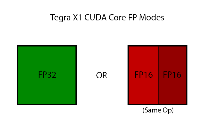
The Gflops reported are a little confusing. If it's a FMA (fused multiply-add) benchmark then you wouldn't expect numbers to quite hit the theoretical peak of the hardware, so I wouldn't necessarily expect nice round power-of-two results. It could also include both CPU and GPU benchmarks. However, it still doesn't really make any sense either from what we know of the Switch hardware, or from the reported Julia results. A 2 SM Maxwell/Pascal GPU at 1005MHz would have a theoretical maximum capability of 515 Gflops, and as far as I'm aware a quad-A57 at 2143MHz would have a theoretical maximum of 137 Gflops (although I'm open to correction on this). It simply wouldn't be possible for the two combined to hit 875 Gflops.

The Gflops also don't make sense when compared to the Julia benchmark results. To get 800fps in that test you'd expect a card somewhere in the 4-5Tflops range, not 875Gflops. Again I suppose you could run the test at 640x480 or something like that, but I can't imagine why someone would set up a benchmark to run at such a low resolution.


The temp differences between idle and load actually make some degree of sense (CPU goes from ~29C to ~56C and GPU from 17C to 65C, it's the battery which only goes up from 21C to 32C). What confuses me is why the temperatures of the CPU and GPU are so different. If they're on the same die we'd expect only a couple of degrees difference, yet we're seeing 10+ degrees, which isn't something you'd see on an SoC. I suspect that the actual device they're testing (whatever it is) has a discrete GPU.

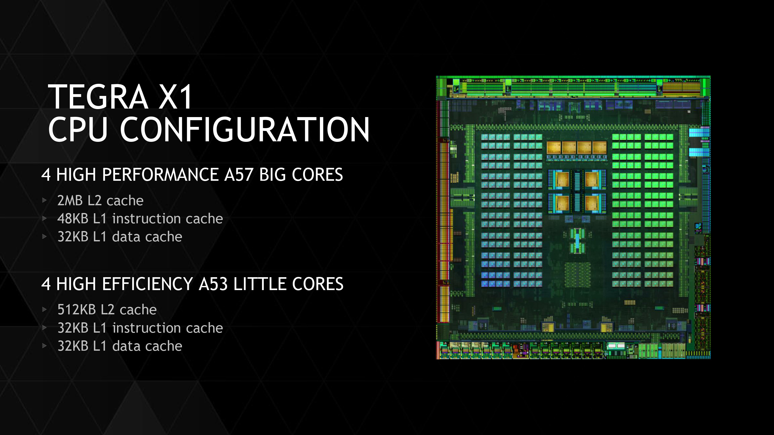
In theory the CPU cores could be split up into separate clusters, but it wouldn't seem to make much sense to do so for Switch, and if they were you would expect cores 0 & 1 and then cores 2 & 3 to be grouped together, not 0 grouped with 3 and 1 with 2.

When you consider that the benchmark indicates that there are 512 CUDA cores, you could theoretically reach 875 GFLOPS. It's possible we've been wrong this whole time, and Nintendo's strategy was to double CUDA cores and clock them lower to save battery life at the expense of die size. All of the leaks we've seen only mention clock speed and we've just been assuming core count to be the same as the Tegra X1.

This is completely hypothetical, but isn't it possible that Nintendo simplified the design (removed A53 cores, CCI-400) and used that space (and then some) to double CUDA core count? It would let them build a powerful handheld that is also energy efficient (still performant at lower clock speeds due to number of cores).

EDIT: Would also explain the 500 man years of engineering that went into this. Simply removing A53 cores and down clocking an X1 wouldn't require 500 man years...
 

AmyS

Member
From what I can tell, a lot of the info gleaned from this thread is uncertain. Is that an accurate assessment?

When can we expect a more detailed and reliable breakdown of the system? Within a week of the system launching?


If Nintendo started with a 20nm chip using Maxwell, they're definitely leaving some room for more powerful and smaller iterations in the future.

Edit: That began to dawn on me as well, these last few weeks, and I totally agree with you.
 

LordOfChaos

Member
I believe in the SCD, and I know Reggie does the PR talk, but he said they know what the competition is doing and they plan to do it a bit different.

Probably if you have your SCD online providing service for Nintendo then you get a discount or you don't have to pay for the online services plus other incentives. I am speculating but that would be a clever way of reducing online infrastructure costs while also rewarding your customers. So for the consumer you gain performance, resolution and other graphical pluses on games while also gaining other rewards, that is a no brainer for most consumers and for Nintendo.

The SCD could also explain why 3rd parties are so quiet right now, or maybe they are just waiting on the launch. I hope it comes true...


My problem with the SCD is that they have nothing with the appropriate bandwidth to do so.

A 1050 hits maybe 85%-90% of its performance on TB3 - that's 40Gb/s. The Switch has USB C 3.0 gen 1, not gen 2, which is 5Gb/s. About 12% of that bandwidth.

Wireless would be even lower bandwidth, AC would peak around 1Gb/s and in the real world would be lower.
 

AmyS

Member
I believe in the SCD, and I know Reggie does the PR talk, but he said they know what the competition is doing and they plan to do it a bit different.

Probably if you have your SCD online providing service for Nintendo then you get a discount or you don't have to pay for the online services plus other incentives. I am speculating but that would be a clever way of reducing online infrastructure costs while also rewarding your customers. So for the consumer you gain performance, resolution and other graphical pluses on games while also gaining other rewards, that is a no brainer for most consumers and for Nintendo.

The SCD could also explain why 3rd parties are so quiet right now, or maybe they are just waiting on the launch. I hope it comes true...


My problem with the SCD is that they have nothing with the appropriate bandwidth to do so.

A 1050 hits maybe 85%-90% of its performance on TB3 - that's 40Gb/s. The Switch has USB C 3.0 gen 1, not gen 2, which is 5Gb/s. About 12% of that bandwidth.

Wireless would be even lower bandwidth, AC would peak around 1Gb/s and in the real world would be lower.

What about simply using GeForce Now, instead of releasing a physical SCD box at retail, is there any technical reason Switch could not use/access GeForce Now, provided a user has at least 25 Gbps internet, like PCs/Mac will be able to play games making use of GTX 1060 or GTX 1080 (for fewer minutes/credit time) ?
 

blu

Wants the largest console games publisher to avoid Nintendo's platforms.
What about simply using GeForce Now, instead of releasing a physical SCD box at retail, is there any technical reason Switch could not use/access GeForce Now, provided a user has at least 25 Gbps internet, like PCs/Mac will be able to play games making use of GTX 1060 or GTX 1080 (for fewer minutes/credit time) ?
The #1 issue with remote play is not BW, it's latency.
 

LordOfChaos

Member
What about simply using GeForce Now, instead of releasing a physical SCD box at retail, is there any technical reason Switch could not use/access GeForce Now, provided a user has at least 25 Gbps internet, like PCs/Mac will be able to play games making use of GTX 1060 or GTX 1080 (for fewer minutes/credit time) ?

Well, then you're using Geforce Now, and the Switch as a device becomes pointless. They're also unable to physically eliminate all the latency game streaming has, making physical consoles still the way for a while.

As for additive processing, well, lets look to Microsoft to see how that turned out...The Cloud™ can add mostly asynchronous CPU work that aren't frame sensitive, but most GPU work is.

That's also 25x what Google Fibre offers at 1Gb/s :p
 

Osiris

I permanently banned my 6 year old daughter from using the PS4 for mistakenly sending grief reports as it's too hard to watch or talk to her
Tell me what country is offering 25Gb/s Internet, because I'm emigrating if so! :p
 
Right, 100 is 10^2, and 121 is 11^2, so it takes a sole mm measurement/estimate error to misjudge a 121mm^2 die for a 100mm^2 die.

Indeed, such a person should see the memory markings clearly.

Does this make you think that the leaker is fabricating some things, or that these components were covered for some reason?

Traditionally PCB versions would be clearly indicated in most industries, but in nintendo's case you might need to know their internal coding monikers.

BTW, after taking a second round of glances at the teardown images, it's pretty obvious nintendo intend to provide larger eMMC SKUs in the future, as the entire eMMC is on a flippable connector. Actually, it might be even semi-servicable by users, as long as they are willing to take apart their switches.

That's a good point and that makes a lot of sense. A 64GB (or higher) revision might come within the next couple years.

ed: Since apparently it's my evening for revisiting data sources, glancing at the TX1 whitepaper, a curious claim pops out - nv claim their A57 is 1.4x more performant per the same power levels as Exynos 5433. Which is quite a bold statement to make for the exact-same uarch cores.

As per the extraordinary-high flops from the Julia shots - could it be the bench was built for fp16?

Doesn't the benchmark readout explicitly specify single and double precision performance? Rather than half precision?

When you consider that the benchmark indicates that there are 512 CUDA cores, you could theoretically reach 875 GFLOPS. It's possible we've been wrong this whole time, and Nintendo's strategy was to double CUDA cores and clock them lower to save battery life at the expense of die size. All of the leaks we've seen only mention clock speed and we've just been assuming core count to be the same as the Tegra X1.

This is completely hypothetical, but isn't it possible that Nintendo simplified the design (removed A53 cores, CCI-400) and used that space (and then some) to double CUDA core count? It would let them build a powerful handheld that is also energy efficient (still performant at lower clock speeds due to number of cores).

EDIT: Would also explain the 500 man years of engineering that went into this. Simply removing A53 cores and down clocking an X1 wouldn't require 500 man years...

Well the photos in the OP show a 121mm^2 die, which is apparently the same size as a TX1. Based on the TX1 floorplans shared a couple pages back* the removal of the A53s would allow very few extra CUDA cores to be added. Maybe 4-8 at most?

So I have no idea where they could have fit an extra 256, unless the die in the OP isn't the final retail one. Though, even the Foxconn leak claimed about 10x10mm, so I don't really see how it's even theoretically possible to fit 512 CUDA cores in there.

*EDIT: This image-

X1-CPU.jpg
 

Vena

Member
Tell me what country is offering 25Gb/s Internet, because I'm emigrating if so! :p

The Country of Vena offers 100 Tb/s speeds. But only has a citizen of one and a total diameter of about a third of a meter. We have a strict immigration policy of one in, one out.
 

buttdiver

Member
When you consider that the benchmark indicates that there are 512 CUDA cores, you could theoretically reach 875 GFLOPS. It's possible we've been wrong this whole time, and Nintendo's strategy was to double CUDA cores and clock them lower to save battery life at the expense of die size. All of the leaks we've seen only mention clock speed and we've just been assuming core count to be the same as the Tegra X1.

This is completely hypothetical, but isn't it possible that Nintendo simplified the design (removed A53 cores, CCI-400) and used that space (and then some) to double CUDA core count? It would let them build a powerful handheld that is also energy efficient (still performant at lower clock speeds due to number of cores).

EDIT: Would also explain the 500 man years of engineering that went into this. Simply removing A53 cores and down clocking an X1 wouldn't require 500 man years...

The benchmark is fake, and there aren't 512 CUDA cores.
 

OryoN

Member
For me personally, I'm already impressed at what is possible on the Switch. Prior to the January reveal, I kinda held my breath possibly waiting to be dissappointed by what I'd see. Once ARMS began running actual gameplay, it was actually a relief! It was considerably better than what I had expected, the vibrant colors, good lighting/shading, the fluidity of animation - even clothing - and of course, a smooth 60fps! I thought; "It's no PS4, but clearly, this is a pretty capable system, despite its size!" This was all out of the gate, likely spent most of its days on development hardware that was a step down from the final version. I expect some really impressive stuff further down the line.

This makes me all the more curious to know what's under the hood. Or what's the reason for all the devs enthusiasm(both on and "off" camera). I'm not sure I can be disappointed at this point. But I can't speak for anyone else. I will either be very confused(really great performance from seemingly "weak" specs). Or things may make more sense as to why this tiny machine performs the way it does, even in this very early stage in its life. Only a few more days...

With that, I'll be in spectator mode from here on out(unless I really must respond).
 

blu

Wants the largest console games publisher to avoid Nintendo's platforms.
Does this make you think that the leaker is fabricating some things, or that these components were covered for some reason?
From the teardown shots, the memory devices are clearly not obfuscated by any substance, and IFF that's the actual case on the consumer units I'd really have no clue how the part number bit could escape someone. Now, consumer SKU _could_ have its ram devices partially covered in epoxy to prevent, erm, tampering, which _could_ obfuscate the part numbers. Another possibility is memory made contact with the heat-conducting plate, and had thermal paste residue.

Doesn't the benchmark readout explicitly specify single and double precision performance? Rather than half precision?
What the readings say and what was actually run might not need exactly match. In most GLES shaders it takes a single line of code to turn all computations from fp32 to fp16 or vice versa.
 

Inuhanyou

Believes Dragon Quest is a franchise managed by Sony
Nintendo will sell more Switches in the first month than Nvidia has sold for all the Shield devices combined lifetime to date. It's a huge win for the Tegra Team and it will definitely keep Nvidia invested with furthering low power tech.

it would benefit both parties if Nvidia and Nintendo continued their synergistic effect far into the future. Atleast now Nvidia is not all "consoles DOOMED" anymore
 
From the teardown shots, the memory devices are clearly not obfuscated by any substance, and IFF that's the actual case on the consumer units I'd really have no clue how the part number bit could escape someone. Now, consumer SKU _could_ have its ram devices partially covered in epoxy to prevent, erm, tampering, which _could_ obfuscate the part numbers. Another possibility is memory made contact with the heat-conducting plate, and had thermal paste residue.


What the readings say and what was actually run might not need exactly match. In most GLES shaders it takes a single line of code to turn all computations from fp32 to fp16 or vice versa.

Interesting, thanks. I wonder if the test was coded in a way that effectively doubled the CUDA core count to account for the double speed FP16 processing.
 
What the readings say and what was actually run might not need exactly match. In most GLES shaders it takes a single line of code to turn all computations from fp32 to fp16 or vice versa.
Come to think of it, wouldn't FP16 effectively give twice the logical cores, sort of like how hyperthreading makes Windows show you have twice as many cores as you actually have? That could perhaps explain the core count in that picture.
 

LordOfChaos

Member
Come to think of it, wouldn't FP16 effectively give twice the logical cores, sort of like how hyperthreading makes Windows show you have twice as many cores as you actually have? That could perhaps explain the core count in that picture.

No, FP16 refers to half precision GPU operations in this benchmark, not CPU.

GCC supports half precision on ARM, but the system would not see this as doubling the CPU cores.
 

defferoo

Member
Well the photos in the OP show a 121mm^2 die, which is apparently the same size as a TX1. Based on the TX1 floorplans shared a couple pages back* the removal of the A53s would allow very few extra CUDA cores to be added. Maybe 4-8 at most?

So I have no idea where they could have fit an extra 256, unless the die in the OP isn't the final retail one. Though, even the Foxconn leak claimed about 10x10mm, so I don't really see how it's even theoretically possible to fit 512 CUDA cores in there.

*EDIT: This image-

True, again, what I said was completely hypothetical. The SDK leaks explicitly state it has 256 CUDA cores, so that benchmark is most likely fake.
 

LordOfChaos

Member
I know, but we were operating under the assumption the CPU and GPGPU cores were being added together (4+512=516)

I'm not quite sure which you're asking then. FP16 making 512 shaders out of 256?

FP16 wound't double CUDA cores either, it works as two FP16 instructions within one op. System still sees one CUDA core and loads it with two FP16 instructions.

FP16Op.png


Anyways that benchmark also shows the correct 4 cores, I'm not sure the "516 Core ARMv8" means 516 cores so much as a core type maybe? I don't see why GPU cores would be listed before "ARMv8"
 
I know, but we were operating under the assumption the CPU and GPGPU cores were being added together (4+512=516)

Right, the benchmark may have been programmed to essentially count the 256 CUDA cores twice to account for the 2x FP16 processing giving us 256*2 + 4 = 516.

True, again, what I said was completely hypothetical. The SDK leaks explicitly state it has 256 CUDA cores, so that benchmark is most likely fake.

It does look odd, but there's a chance it's legit as we're discussing above. But I don't see how 512 CUDA cores could be physically possible in that space. And again there's no guarantee that the hardware referred to in the SDK leak is the retail hardware, though it's looking like 256 CUDA cores is essentially confirmed.
 
I'm not quite sure which you're asking then. FP16 making 512 shaders out of 256?

FP16 wound't double CUDA cores either, it works as two FP16 instructions within one op. System still sees one CUDA core and loads it with two FP16 instructions.

FP16Op.png
Yes, that's what I was talking about. GPU cores generally operate in parallel (in small groups) on the same operations to begin with. FP16 effectively doubles the number of "cores" in each group, logically but not physically. (One core working with two FP16 values at a time instead of one FP32 value.) Unless I'm totally misreading this.
 

LordOfChaos

Member
Yes, that's what I was talking about. GPU cores generally operate in parallel (in small groups) on the same operations to begin with. FP16 effectively doubles the number of "cores" in each group, logically but not physically. (One core working with two FP16 values at a time instead of one FP32 value.) Unless I'm totally misreading this.

That's right, maybe I'm just unfamiliar with the benchmark though but from a system and scheduler level things would still look like the same number of CUDA cores, just with two merged FP16 ops rather than one FP32 op. More like, I guess, micro op fusion, than hyperthreading.
 
That's right, maybe I'm just unfamiliar with the benchmark though but from a system and scheduler level things would still look like the same number of CUDA cores, just with two merged FP16 ops rather than one FP32 op. More like, I guess, micro op fusion, than hyperthreading.

Right, hyperthreading was just the only example I could think of with a reported difference between logical and physical cores, I didn't mean to imply that the Tegra GPUs used hyperthreading.

I guess the thing I'm still unsure about with regard to FP16 is whether it shoves through twice as many floating point values in a single op or twice as many ops in a single cycle. I was assuming it was the former (especially because doing two ops in a cycle won't guarantee double performance unless there are no dependencies between the ops in question).
 

AzaK

Member
I think if they decided to go with Maxwell instead of Pascal that's a really bad decision, Pascal would improve battery life and heat, which is really important for a "portable".

I really hope it's Pascal, even if it's a custom version of X1 instead of X2.

Well I doubt it'd affect sales and they can move to that later.


Does it really matter with a battery life of ~20 hours? Even if it took 8 hours, you gotta sleep for a couple hours at some point.

General use no but I can't remember the number of time my DualShock 4 has run out of batteries on me. I have children, they don't reliably put controllers on to charge when they're finished :)
 

KingSnake

The Birthday Skeleton
So I looked back over the Foxconn leak translation here http://www.neogaf.com/forum/showpost.php?p=229879660&postcount=836

Checking this again, the leaker was totally wrong about the screen. From resolution to brightness. Also reading through it seems like he put together what he saw through the factory with some bits that he heard from colleagues and with some educated guesses to fill the gaps.

Like he had partial access to a test bench and saw the a teared-down Switch (no battery, connected to some shitty test screen and could see the SoC close enough to see the resemblance to a Nvidia SoC and estimate the size of it, but not close enough to read the memory model or type. And saw the benchmark running on that (with what seems to be max-out clocks that could work also on a custom X1 that has no heat or power consumption limitation imposed on it).

Then he clearly had access to the manufactured Switch itself, considering all the other info provided, including joycons, weight (btw, does the weight fit?) and battery capacity (which is printed on it).

A lot of the rest seems a combination of hearsay and speculation.

I still question the bit about 16nm, seems mentioned only once about the standard unit and in passing, I wonder if it's not also speculation or something he expected to just be like this, considering other devices manufactured there.
 

Thraktor

Member
Thanks. It's interesting, just wish it had more context to it (maybe it does, just don't know chinese) so we can get a clearer picture of what's being claimed here, it just seemed to have been dropped on here out of the blue. I guess (if this was real) they'd do that Julia benchmark at 480x360 specifically to stress test the CPU?

The benchmark is explicitly designed to stress the GPU, so it should barely touch the CPU at all. There's technically nothing stopping someone from choosing to run the test at whatever resolution they want, it just seems strange to run it at a resolution so low.

By the by, a largely tangential anecdote, as I'm as A57-less as the next guy, but it just struck me to check, and _some_ of the 28nm A53s I have access to tend to idle (read: min clock) at 312MHz. Just found that fact rather curious in the context of that shot.

It did occur to me that it seemed like an unusually low idle speed for A57s, although if it's not Switch it doesn't hugely matter.

So I looked back over the Foxconn leak translation here http://www.neogaf.com/forum/showpost.php?p=229879660&postcount=836

A couple things jump out at me. First, the size of the "CPU" (I assume he means SoC) is about 10mm^2, which is likely a typo/misunderstanding meaning 100mm^2, close to what we have determined in this thread (121mm^2 right?) but a bit smaller.

He also says he can see the two memory chips but not the model or type. Wouldn't that be visible to someone who can see the actual components on the motherboard, as we can see in the OP?

He may well have seen and been able to read the RAM modules, but just seeing a series of alphanumeric codes doesn't mean he can figure out the critical info. He quite obviously couldn't take a photo of them, or search the product codes on any company computers, and even writing down the codes on a scrap of paper would probably be risky. He could try to memorise SEC531 K4F6E30 4HBMGCH and figure it out when he got home, but he'd have to have a far better memory than me to pull that off.

Finally, he makes a comment that makes little sense to me:


What kind of differences would be noticeable on a different motherboard? Various numbers printed on the board?

There may have been a slight change to the layout of the board, or a couple of components swapped over for newer versions. It wouldn't surprise me if PCBs like this went through a few iterations running up to final manufacturing (and sometimes even after).

Anyway, I still don't get why people are somehow dismissing the Foxconn clocks/conclusion that it could be 16nm based on the photos in the OP. All we can see in these figures is the size of the SoC, and as I understood it 16nm chips don't get much (if any) increased density over 20nm, so they would look the same, right down to the size, right?

I wouldn't dismiss it from the photo (as you say it would be a virtually identical size), I just think it's unlikely based on the Eurogamer clock speed leaks. I still wouldn't completely rule it out, though.

BTW, after taking a second round of glances at the teardown images, it's pretty obvious nintendo intend to provide larger eMMC SKUs in the future, as the entire eMMC is on a flippable connector. Actually, it might be even semi-servicable by users, as long as they are willing to take apart their switches.

I mentioned that a few pages back, but eMMC modules are inherently swappable by design, so you don't need break-out boards to accommodate different capacities (see almost every smartphone). I had speculated that they may have it there to accommodate the possibility of switching to eUFS, but to be honest looking at the mainboard I think it's most likely that they simply couldn't fit it in any other way.

ed: Since apparently it's my evening for revisiting data sources, glancing at the TX1 whitepaper, a curious claim pops out - nv claim their A57 is 1.4x more performant per the same power levels as Exynos 5433. Which is quite a bold statement to make for the exact-same uarch cores.

TX1 has a quite substantial bandwidth advantage over Exynos 5433, so it could be that they were just choosing they benchmarks very carefully. TSMC's 20nm process may outperform Samsung's 20nm as well to some degree.

When you consider that the benchmark indicates that there are 512 CUDA cores, you could theoretically reach 875 GFLOPS. It's possible we've been wrong this whole time, and Nintendo's strategy was to double CUDA cores and clock them lower to save battery life at the expense of die size. All of the leaks we've seen only mention clock speed and we've just been assuming core count to be the same as the Tegra X1.

This is completely hypothetical, but isn't it possible that Nintendo simplified the design (removed A53 cores, CCI-400) and used that space (and then some) to double CUDA core count? It would let them build a powerful handheld that is also energy efficient (still performant at lower clock speeds due to number of cores).

EDIT: Would also explain the 500 man years of engineering that went into this. Simply removing A53 cores and down clocking an X1 wouldn't require 500 man years...

If the SoC we're looking at in this thread is the final one, then there's zero chance that they've gone with 512 cores, they literally wouldn't be able to fit a GPU like that in a 120mm² SoC. Even if it's not then I'd still put the chances as very low.

The 500 man years were never said to focus entirely on the SoC. They almost certainly include software development, and could well include other things like cooling design, etc.

Well the photos in the OP show a 121mm^2 die, which is apparently the same size as a TX1. Based on the TX1 floorplans shared a couple pages back* the removal of the A53s would allow very few extra CUDA cores to be added. Maybe 4-8 at most?

So I have no idea where they could have fit an extra 256, unless the die in the OP isn't the final retail one. Though, even the Foxconn leak claimed about 10x10mm, so I don't really see how it's even theoretically possible to fit 512 CUDA cores in there.

*EDIT: This image-

Just an FYI, but this isn't actually an accurate representation of the TX1, Nvidia just puts out these renderings to show how many "cores" their GPUs and SoCs have. As a point of reference, here's what a GP104 actually looks like:


You can actually count the 20 SMs around the chip quite easily, and Switch's SoC should have two SMs (we think) which look pretty similar.

There are lots more die photos by the same guy here, by the way, he does an extremely good job considering he does the entire thing at home as a hobby.

What the readings say and what was actually run might not need exactly match. In most GLES shaders it takes a single line of code to turn all computations from fp32 to fp16 or vice versa.

Strictly speaking the shader code is GLSL for Julia (not that it matters), but whoever's written the shell script has written the output as single-precision, which seems a very strange thing to do if they've also gone in and changed the code to FP16. Particularly so as they've got a separate double-precision line still there, as opposed to doing both a half-precision and single-precision run, which may make sense on an architecture like this.
 
Checking this again, the leaker was totally wrong about the screen. From resolution to brightness. Also reading through it seems like he put together what he saw through the factory with some bits that he heard from colleagues and with some educated guesses to fill the gaps.

Like he had partial access to a test bench and saw the a teared-down Switch (no battery, connected to some shitty test screen and could see the SoC close enough to see the resemblance to a Nvidia SoC and estimate the size of it, but not close enough to read the memory model or type. And saw the benchmark running on that (with what seems to be max-out clocks that could work also on a custom X1 that has no heat or power consumption limitation imposed on it).

Then he clearly had access to the manufactured Switch itself, considering all the other info provided, including joycons, weight (btw, does the weight fit?) and battery capacity (which is printed on it).

A lot of the rest seems a combination of hearsay and speculation.

I still question the bit about 16nm, seems mentioned only once about the standard unit and in passing, I wonder if it's not also speculation or something he expected to just be like this, considering other devices manufactured there.

Yeah that makes sense, though the screen brightness comment is highly subjective and could be just in comparison to high end smartphones and tablets. I think he nailed the weight pretty closely too based on Nintendo's official specs.

He may well have seen and been able to read the RAM modules, but just seeing a series of alphanumeric codes doesn't mean he can figure out the critical info. He quite obviously couldn't take a photo of them, or search the product codes on any company computers, and even writing down the codes on a scrap of paper would probably be risky. He could try to memorise SEC531 K4F6E30 4HBMGCH and figure it out when he got home, but he'd have to have a far better memory than me to pull that off.

You'd think with his level of knowledge and experience he would at least know they were Samsung modules if he saw the writing. It's just interesting that he explicitly mentioned he wasn't able to identify it. It could be as KingSnake said above that he just wasn't able to look closely enough at it.


There may have been a slight change to the layout of the board, or a couple of components swapped over for newer versions. It wouldn't surprise me if PCBs like this went through a few iterations running up to final manufacturing (and sometimes even after).

Hmm that's interesting, so it could be that he has seen some pre-final retail units, or possibly the motherboard might differ between different retail units? I wonder if the unit in the OP has one of the older or newer motherboards. I guess only the leaker would be able to tell us that

Just an FYI, but this isn't actually an accurate representation of the TX1, Nvidia just puts out these renderings to show how many "cores" their GPUs and SoCs have. As a point of reference, here's what a GP104 actually looks like:

You can actually count the 20 SMs around the chip quite easily, and Switch's SoC should have two SMs (we think) which look pretty similar.

There are lots more die photos by the same guy here, by the way, he does an extremely good job considering he does the entire thing at home as a hobby.

Oooh that's a really cool image, thanks! As someone who studied materials science that's a fascinating picture, it really shows the value of space and creative mask production.

And yeah I figured the other image wasn't exactly what it would look like but it is a fair representation of the various component sizes, right?
 

AmyS

Member
People just hoping against hope that the Switch custom Tegra has:

-512 GPU cuda cores (na, it's going to be 256)

-600 Gflops to 1 TF (nope, it's going to be right around ~393 Gflops (fp32) when docked and 157 Gflops (fp32) undocked as a portable
-That FP16 capability somehow doubles the performance (it won't, could be useful in some situations of rendering but that will take time to utilize, give it a few generations of software)

- Pascal GPU architecture (probably not, it's gonna be Maxwell, but there's not a whole lot of difference between Maxwell 2.0 and Pascal anyway)
- 128-bit bus for 50 GB/sec bandwidth (nope, it's going to be 64-bit and ~25 GB/sec)

- Denver2 or A72 CPU cores (it's gonna be four A57s).

- 16nm FinFET (unlikely, probably 20nm)

- Maybe even simply, somewhat higher CPU and/or GPU clock speeds from what Eurogamer leaked.

I feel that a small clock speed bump from those July dev kits is the only fairly reasonable possibility.
 

Zil33184

Member
People just hoping against hope that the Switch custom Tegra has:

-512 GPU cuda cores (na, it's going to be 256)

-600 Gflops to 1 TF (nope, it's going to be right around ~393 Gflops (fp32) when docked and 157 Gflops (fp32) undocked as a portable
-That FP16 capability somehow doubles the performance (it won't, could be useful in some situations of rendering but that will take time to utilize, give it a few generations of software)

- Pascal GPU architecture (probably not, it's gonna be Maxwell, but there's not a whole lot of difference between Maxwell 2.0 and Pascal anyway)
- 128-bit bus for 50 GB/sec bandwidth (nope, it's going to be 64-bit and ~25 GB/sec)

- Denver2 or A72 CPU cores (it's gonna be four A57s).

- 16nm FinFET (unlikely, probably 20nm)

- Maybe even simply, somewhat higher CPU and/or GPU clock speeds from what Eurogamer leaked.

I feel that a small clock speed bump from those July dev kits is the only fairly reasonable possibility.

Also people tend to be overly favourable in comparisons to GCN in XBO and PS4. I think someone assumed 40% performance advantage over a comparable GCN part, which is just unsubstantiated fudge factoring. Given how well AMD parts perform on Vulcan optimised games, the "Nvidia vs. AMD flops" argument may not have any bearing on console.

The other issue is that docked mode may not provide a substantial boost in games that are already using the max bandwidth mode.

To me the most optimistic scenario will be Shield Android TV level performance with the thin OS and API offsetting some of the performance loss from the decreased clock speed.
 

Polygonal_Sprite

Gold Member
That was LCGeek. She stated after the Eurogamer story that they had the chipset correct, but she didn't know that they would clock them so low. Despite her constantly saying that it may be subject to change due to numerous factors even prior to that story, she got banned after the January 13th event.

Is LCGeek permanently banned? If so were they banned on that particular day because of what was shown at the event? Same goes for Nate Drake.
 
Here is a question. Miyamoto said they knew they messed up with Wii U's CPU. He said they would fix this mistake next go round (Switch). How does using 3 underclocked A57's help? Is it that much better a solution then what Wii U had compared to XB1 and PS4?

I don't recall Miyamoto directly saying that about the CPU, but he did indirectly referenced it when he discussed Pikmin and Star Fox as a bottleneck. Was it something else he recently said?

Anyway, it is much better. It didn't help that the CPU in the Wii U was based on the EOL IBM G3 architecture and had no future.
If the Eurogamer leak is true: 3 cores @1Ghz, in both docked and hanheld, it looks really weak indeed.
While A72 would be better, A57 are close to a match to the Jaguars in the PS4 despite the clock difference. That is not remotely close to the situation with the Wii U's CPUs.

People just hoping against hope that the Switch custom Tegra has:

-512 GPU cuda cores (na, it's going to be 256)

-600 Gflops to 1 TF (nope, it's going to be right around ~393 Gflops (fp32) when docked and 157 Gflops (fp32) undocked as a portable
-That FP16 capability somehow doubles the performance (it won't, could be useful in some situations of rendering but that will take time to utilize, give it a few generations of software)

- Pascal GPU architecture (probably not, it's gonna be Maxwell, but there's not a whole lot of difference between Maxwell 2.0 and Pascal anyway)
- 128-bit bus for 50 GB/sec bandwidth (nope, it's going to be 64-bit and ~25 GB/sec)

- Denver2 or A72 CPU cores (it's gonna be four A57s).

- 16nm FinFET (unlikely, probably 20nm)

- Maybe even simply, somewhat higher CPU and/or GPU clock speeds from what Eurogamer leaked.

I feel that a small clock speed bump from those July dev kits is the only fairly reasonable possibility.

I believe most people will be ok with Eurogamer's numbers at this point, though they would want more if it's possible. The Foxconn's rumor/leak is definitely interested and shouldn't be completely discredited yet.
 

EloquentM

aka Mannny
People just hoping against hope that the Switch custom Tegra has:

-512 GPU cuda cores (na, it's going to be 256)

-600 Gflops to 1 TF (nope, it's going to be right around ~393 Gflops (fp32) when docked and 157 Gflops (fp32) undocked as a portable
-That FP16 capability somehow doubles the performance (it won't, could be useful in some situations of rendering but that will take time to utilize, give it a few generations of software)

- Pascal GPU architecture (probably not, it's gonna be Maxwell, but there's not a whole lot of difference between Maxwell 2.0 and Pascal anyway)
- 128-bit bus for 50 GB/sec bandwidth (nope, it's going to be 64-bit and ~25 GB/sec)

- Denver2 or A72 CPU cores (it's gonna be four A57s).

- 16nm FinFET (unlikely, probably 20nm)

- Maybe even simply, somewhat higher CPU and/or GPU clock speeds from what Eurogamer leaked.

I feel that a small clock speed bump from those July dev kits is the only fairly reasonable possibility.
i have no idea why people keep making these posts about phantom gaffers making switch dream lists. No one here is expecting any of this. It's speculation at most.
 

Buggy Loop

Member
6hN3U.jpg


Peoples expecting pure TX1 and then stop speculating are boring. With a few weeks or a month at most of opening the whole thing open, the retail unit that is, it's good fun to roll the dices, even if odds are low.

those 500 man years!
 

dahuman

Neo Member
6hN3U.jpg


Peoples expecting pure TX1 and then stop speculating are boring. With a few weeks or a month at most of opening the whole thing open, the retail unit that is, it's good fun to roll the dices, even if odds are low.

those 500 man years!

can you blame us after the wii u?
 
Top Bottom