• Hey, guest user. Hope you're enjoying NeoGAF! Have you considered registering for an account? Come join us and add your take to the daily discourse.

AMD reveals 'Polaris' next-gen graphics architecture

mocoworm

Member
http://www.eurogamer.net/articles/digitalfoundry-2016-amd-reveals-polaris-next-gen-graphics-hardware

https://youtu.be/5g3eQejGJ_A

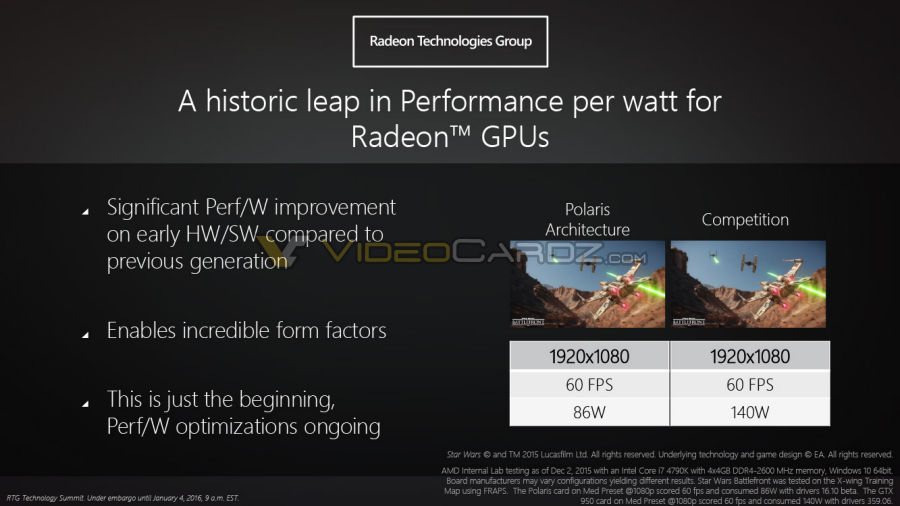
AMD today revealed its new fourth generation GCN architecture, dubbed Polaris, offering a substantial leap in power and efficiency. Comparing an unannounced GPU product against the Nvidia's GTX 950 running Star Wars Battlefront at medium settings at 1080p60, AMD says that its new architecture offers a 61 per cent reduction in power consumption, requiring 84W vs Nvidia's 140W.

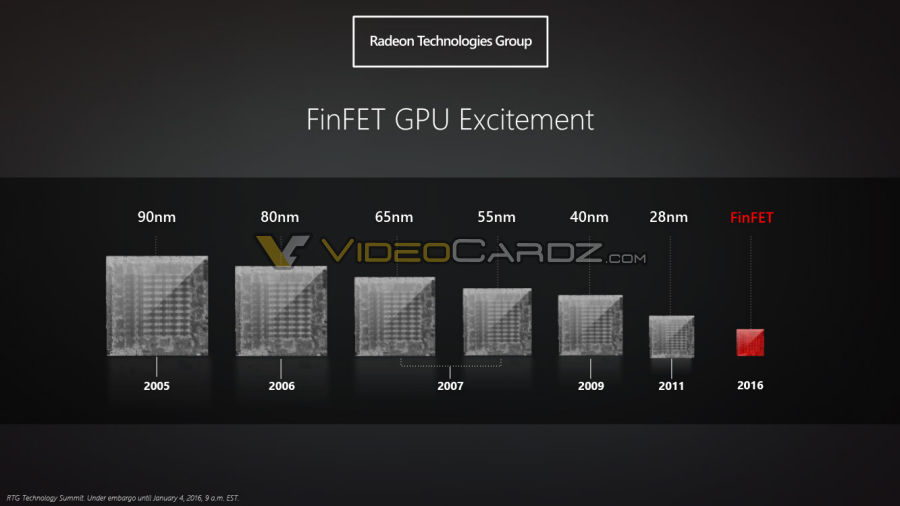
Since 2011, both companies have used 28nm production - meaning that each transistor on the chip is one billionth of a metre long. While the process has been refined since then, it's fair to say that both companies had hit a brick wall in getting more out of the existing technology. This year, moving to a 16nm 'FinFET' process is finally possible - with the larger planar transistors of the old process giving way to the smaller '3D' transistors in the new production technology.

So what does that mean for gamers? The bottom line is simple: GPUs comparable with the current generation can be smaller and more power efficient - as AMD is attempting to demonstrate with its Polaris vs GTX 950 Battlefront comparison. But more to the point, this also means that larger chips with the same levels of power consumption as existing GPUs can pack on far, far more transistors, meaning much more processing power.

We were sent this information way ahead of time, and AMD isn't giving anything specific away with regards its plans for Polaris in terms of actual Radeon products, but more details may emerge as the Consumer Electronics Show (CES) progresses in Las Vegas. We've embedded the complete presentation AMD supplied below:

https://www.youtube.com/watch?v=5g3eQejGJ_A

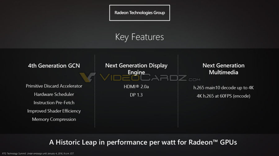
So what do we know? The fourth generation of the GCN architecture features extensive improvements, including a primitive discard accelerator, hardware scheduler, instruction pre-fetch, improved shader efficiency and better memory compression. AMD catches up with Nvidia with support for HDMI 2.0a, plus there's DisplayPort 1.3 compatibility. Media functions are bolstered with support for the HEVC codec - we're promised real-time onboard encoding at 4K60. We expect that decode also follows that spec too (as the Fury products support it already).

But it's the massively improved power efficiency that is compelling here: AMD reckons that Polaris is going to mean big things gaming notebooks, small form factor desktops and full-on graphics card with less onerous power requirements (and fewer power connectors). It has specifically targeted 'console calibre' performance for 'thin and light' laptops - great news, bearing in mind that PS4 and Xbox One define the baseline for most modern triple-A titles. The ability to have that kind of performance in smaller form factor notebooks can only be a good thing.

Polaris GPUs are planned for release in Q2 this year, meaning that the earliest we'll see them is April. We expect to see Nvidia's rival tech - codenamed Pascal - to arrive in the same time window. We're particularly interested in seeing the higher-end products from both firms that should be paired with HBM memory technology - but the recent reveal of higher bandwidth GDDR5X also gives AMD and Nvidia new VRAM options for their next-gen graphics technology. On top of that, we should see more utilisation of DirectX 12, meaning even higher levels of performance - exactly what we need with the upcoming arrival of high-end virtual reality in the same timeframe.


http://videocardz.com/58031/amd-announces-polaris-architecture-gcn-4-0

AMD Polaris vs NVIDIA Pascal

Polaris is new codename for 14nm FinFET architecture that will be introduced with new graphics cards later this year. From what I’ve heard, AMD is planning to launch first Radeon 400 cards in the summer. Even though the launch is still months ahead, the company decided to share more details about their future portfolio to tease gamers (and probably investors).

To give you a perspective, this is how Polaris fits after 28nm architecture.

2011 — 28nm GCN 1.0 — Tahiti / Cape Verde
2013 — 28nm GCN 2.0 — Hawaii / Bonaire
2015 — 28nm GCN 3.0 — Fiji / Tonga
2016 — 14nm FinFET Polaris (GCN 4.0)


In the last 10 years fabrication process shrunk significantly (in 2005 it was 90nm). Obviously smaller node means higher power efficiency and therefore higher performance at lower power consumption. Unfortunately the slides are not very accurate, in fact they don’t even have any numbers, so I can’t share more details as of yet.

The GPU design was modified to include new logical blocks. What’s new is Command Processor, Geometry Processor, Multimedia Cores, Display Engine and upgraded L2 Cache and Memory Controller.

Last but not least, the new architecture has 4th Generation Graphics Core Next Compute Units (aka. GCN 4.0).

AMD Polaris will compete against NVIDIA’s Pascal architecture. Both are believed to utilize High-Bandwidth-Memory 2 (HBM2).

AMD-Polaris-Architecture-2.jpg


Might be cool, depending on price and whether the drivers/companion software is unfucked. Kinda interested to see what Pascal will bring to the table to compete with Polaris.
 

mrklaw

MrArseFace
the first video ends with a little battlefront comparison. I like lower watts, but it was only running 1080p/60 at medium settings. I hope more performance per watt doesn't just mean good news for lower wattage cards - I want more performance at high watts too.
 
Sadly Gameworks titles will kill the performance anyway :/

Beyond this being wildly OT and possibly derailing, it is also inaccurate describing how most gameworks titles actually work (i.e. have tunable and tweakable gameworks variables).
-----
I am curious how many power/perf games are due to the shrink vs. architectural advancements, the comparison they provide with a 950 is somewhat... odd...
 

Kayant

Member
Beyond this being wildly OT and possibly derailing, it is also inaccurate describing how most gameworks titles actually work (i.e. have tunable and tweakable gameworks variables).
-----
I am curious how many power/perf games are due to the shrink vs. architectural advancements, the comparison they provide with a 950 is somewhat... odd...

Yh in the video they do say it's a "comparable" GPU to it though.

Edit -

If am not wrong in saying 950 probably has the best perf/watt in maxwell so I could guess they are trying to show the improvements at their best.
 

jmga

Member
A big part of DX12/Vulcan is offloading what would traditionally be driver work onto middleware developers... so I guess we hope Epic makes good use of it ;)

I know, but all my current games and most over the next few years will be DX9-11 or even OpenGL, so I would not risk getting an AMD just for a few DX12/Vulkan titles.
 
Yh in the video they do say it's a "comparable" GPU to it though.
I guess. But why compare it to the previous gen NV offering and not your own compariable GPU? It is obvious to anyone who follows GPU tech and who cares at all about this stuff that that comparison is strange and surprisingly unrevealing. A comparison with their own previous "similar GPU" would be much more telling!
 

Renekton

Member
Yh in the video they do say it's a "comparable" GPU to it though.

Edit -

If am not wrong in saying 950 probably has the best perf/watt in maxwell so I could guess they are trying to show the improvements at their best.
I think by "comparable" they mean similar performance (Bfront 60fps at 1080p medium), so the demo's purpose is to show die size and power savings for the same performance.
 
Wow, that first image really highlights how badly things have been stalled at 28nm. Really looking forward to the new 14/16nm GPUs (and CPUs) later this year.
 

AmyS

Member
GCN 4.0? NX GPU confirmed!

It would be a really good start for NX if all three devices from the recent Nintendo patents (a.) console, (b.) supplemental computing device and (c.) handheld, all had APUs with GPUs based on Polaris architecture. Even though that alone says nothing about the actual performance level of any of them.
 

Akuun

Looking for meaning in GAF
Please be good.

Please don't have finnicky bullshit software that has random frame hitching unless it has a bunch of game-specific fixes because it's a popular game.
 

Irobot82

Member
Please be good.

Please don't have finnicky bullshit software that has random frame hitching unless it has a bunch of game-specific fixes because it's a popular game.

You're in luck because the current cards don't even do that.
 
Wow really nice power efficiency improve after GTX 950. But hope we can see 2X or more GPU power than before. Like R9 390 price with R9 490 but 2X GPU power and 2X lower power consuming...

Am i doing right. :p
 
This is so cool. I remember the buzz around PS3 and XBox 360 when they were announced to be 90nm. As well as the pc video cards. That seemed to be not so long ago... :(
 

KKRT00

Member
What? 950 is 140W card? How, when 970 is also 140W card.

Going by official TDP from Nvidia, the GTX 950 is 90W card, not 140W.
 

Hellgardia

Member
Cost is also important.
The R7 250 has a TDP of 65W so i would assume system power is also >86W.
If i'm not mistaken the power output shown is for the whole system so that means that you get more than R7 370 level of performance for less power than a R7 250.
I wonder what it's price bracket will be though.
 

Kayant

Member
I think by "comparable" they mean similar performance (Bfront 60fps at 1080p medium), so the demo's purpose is to show die size and power savings for the same performance.

He specifically says GPU though in the video. I think they are just trying to show the efficiency in perf/watt in it's best light and plus Dictator93's point if they used Nano for example it wouldn't appear as much of an improvement.

It's just PR trying to trying to show things at their best. We see this every time with these charts.
 

Amey

Member
I don't understand this comparison.
Surely GTX 950 doesn't consume 140W on it's own. Its TDP is merely 90W.
140W can't be whole system's consumption with i7 4790K. That's too little for gaming.
 

KKRT00

Member
AMD meant "system-power", but wrote "card".
Stupid mistake or intentional bs.

Going by the slide in OP, they were testing it on i7 4970k, so the whole system couldnt operate under the Battlefront's load under 200W.

Seems like BS.

---edit---
Beaten by Amey.
 

tuxfool

Banned
What? 950 is 140W card? How, when 970 is also 140W card.

Going by official TDP from Nvidia, the GTX 950 is 90W card, not 140W.

Read the anandtech article. They were measuring values at the wall and the game is being limited to 60fps thus not stressing the CPU.

This is also probably the most correct way to quickly compare it as Nvidia and AMD measure TDP differently.
 

Locuza

Member
I don't understand this comparison.
Surely GTX 950 doesn't consume 140W on it's own. Its TDP is merely 90W.
140W can't be whole system's consumption with i7 4790K. That's too little for gaming.
It's system-power.
It was 1080p, medium-settings and 60 FPS Limit for Battlefront and the 4790K was limited to 80% power-draw.
Clipboard01.jpg
 

Amaducias

Neo Member
What? 950 is 140W card? How, when 970 is also 140W card.

Going by official TDP from Nvidia, the GTX 950 is 90W card, not 140W.

I don't understand this comparison.
Surely GTX 950 doesn't consume 140W on it's own. Its TDP is merely 90W.
140W can't be whole system's consumption with i7 4790K. That's too little for gaming.

TDP from both Nvidia and AMD on both their sites or powerpoints are never correct.

In this example the GTX 950 doesn't come close to 140W, but a 970 is over 160W.

I prefer checking reviews for the real numbers.
https://www.techpowerup.com/reviews/MSI/GTX_950_Gaming/28.html

it also seems that they're talking about system power in their slides, which might make more sense then, but i'd still take it with a grain of salt.
 

Durante

Member
I honestly hope all the noise about power efficiency (a good thing, mind you) is not indicative of them not having high-end and/or enthusiast class products at the start.
 
This sounds like it would be right up Nintendo's alley, too bad it's likely too new and perhaps expensive (?) to make it into the NX.

It's nice to see a big leap in power consumption like this though, usually all we hear about is POWER!
 

McHuj

Member
For those interested from Anandtech:

As for RTG’s FinFET manufacturing plans, the fact that RTG only mentions “FinFET” and not a specific FinFET process (e.g. TSMC 16nm) is intentional. The group has confirmed that they will be utilizing both traditional partner TSMC’s 16nm process and AMD fab spin-off (and Samsung licensee) GlobalFoundries’ 14nm process, making this the first time that AMD’s graphics group has used more than a single fab. To be clear here there’s no expectation that RTG will be dual-sourcing – having both fabs produce the same GPU – but rather the implication is that designs will be split between the two fabs. To that end we know that the small Polaris GPU that RTG previewed will be produced by GlobalFoundries on their 14nm process, meanwhile it remains to be seen how the rest of RTG’s Polaris GPUs will be split between the fabs.
 

tuxfool

Banned
I honestly hope all the noise about power efficiency (a good thing, mind you) is not indicative of them not having high-end and/or enthusiast class products at the start.

Everything they have said suggests that they're first launching lower end products.

Yields with these new processes will favour smaller dies at the start.
 

Amey

Member
It's system-power.
It was 1080p, medium-settings and 60 FPS Limit for Battlefront and the 4790K was limited to 80% power-draw.

Hmm. This is from techreport review with 5960x running crysis3.
power-load.gif

I guess 140W is doable with 4790k then.
 

Durante

Member
Everything they have said suggests that they're first launching lower end products.

Yields with these new processes will favour smaller dies at the start.
That's what I'm afraid of.

Since I assume both NV and AMD will do that I guess we won't get a real high-end desktop part until the end of the year.
 
Given that the new Finfet node is considerably more expensive, there's no doubt they'll mostly harp about the power efficiency and size. Extra transistors won't be free though, so high end is going to be very expensive, and most likely they'll seriously cut the chip sizes. You can't seriously expect AMD or Nvidia to just make a 600 mm^2 chip right out of the gate. This will no doubt disappoint people who are expecting a new Titan by next summer. More than likely all we get to see this year is a mid-range flagship like the 980 that they'll try to sell for $600.
 
Top Bottom