-
Hey, guest user. Hope you're enjoying NeoGAF! Have you considered registering for an account? Come join us and add your take to the daily discourse.
You are using an out of date browser. It may not display this or other websites correctly.
You should upgrade or use an alternative browser.
You should upgrade or use an alternative browser.
NVIDIA Pascal GPU to feature 17B transistors and 32GB HBM2, coming Q2 2016 (earliest)
- Thread starter Zombie James
- Start date
Goldenmoney
Member
Sounds powerful, but it also sounds expensive as fuck.
Second thing is, Nvidia should have plenty of headroom on 16nm FF+ after Pascal, after finally moving from 28nm to 16nm FF+ - Volta could be to Pascal what Maxwell was to Kepler. A major refresh, not completely new architecture. It's often been said both Pascal and Volta will make use of NV Link.
Perhaps one difference between Pascal and Volta might be Pascal uses HBM2 and Volta uses HBM3 or the Hybrid Memory Cube they originally planned for the Volta intended for 2016.
Pure speculation of course. Feel free to tell me where I'm wrong, as I probably am on some things.or wrong on everything
Speculation is fun.
")
I had to wonder if perhaps Pascal is mostly a shrunk Maxwell whose introduction was a result of the 16nmFF delay, and they wanted to play it safe by using a mature design first ( a bit like Intel's tick-tock*) while making the aforementioned changes/additions (NVLink, HBM, mixed precision) instead of jumping straight to a more significant rejigging on an expensive node. **
I know you mentioned kepler <-> maxwell as not being a major architecture shift, but I consider it to be fairly changed up in a number of ways. IMHO, architecture refresh example would be 750Ti vs 9xx series( or even the GCN series ಠ_ಠ ).
*always hated that the "tick" was the shrunk version of the previous "tock". :|
** i.e. Take tegra x1 GPU, which is Max-based, make it super phat & add/change up a couple things, and shift from 20nm to 16FF+... ¯_(ツ
_/¯Kinda feel like its a long shot that NVLINK will be doable on consumer.
Needs motherboard and CPU to be compliant. Is Nvidia going to go back into the chipset business?I cant see Intel playing nice with them because they are competing companies in the gpgpu space with the Xeon Phi line.
More hoping that they get can get improved multi-gpu scaling as it looks like we are going to need it for Hi-Resolution VR. Seems like that is one of the promises that the silicon interposer offers for multi-die, single card configurations.
I'm just hoping we have a way to do multi-gpu and PCI-E SSD's without compromising bandwidth on the CPU's controller. That might be solvable with Skylake E.
I still feel like my 780TI's run just about everything at 2560x1600. Star Citizen runs flawlessly and that's about the peak of usefully pretty.
Just need to last until Skylake E and the first HBM Titan
I'm still maintaining that NVLink will only be used for servers.
Everything they have said about Nvlink, such as the requirement for special physical connectors makes me think that the protocol requires even stronger signal integrity requirements than PCIE. The physical protocol seems to be be using very high clockspeeds otherwise they wouldn't be worried about the Impedance of connectors used in PCIE. Those preliminary connectors they showed look very much like shielded interfaces used in RF.
This essentially means you cannot just shove in something like a SLI connector unless it is very carefully designed. I could definitely see it being used on Multi Gpu cards though.
Why would they ever cram 17 billion transistors on a chip even if they could? This article doesn't make a lot of sense.
It's a much, much better business strategy to make incremental improvements (maybe 10%/20% improvements tick over tock) and milk it dry. You can go from 8 bil to 10 to 12 to 14 to 18, and you have 4 generations of products to sell rather than 1. Also prevents the consumer from expecting too much because you gave them too good a deal for Pascal.
It's a much, much better business strategy to make incremental improvements (maybe 10%/20% improvements tick over tock) and milk it dry. You can go from 8 bil to 10 to 12 to 14 to 18, and you have 4 generations of products to sell rather than 1. Also prevents the consumer from expecting too much because you gave them too good a deal for Pascal.
They will safely do that once they finished curbstomping AMD into bankruptcy.Why would they ever cram 17 billion transistors on a chip even if they could? This article doesn't make a lot of sense.
It's a much, much better business strategy to make incremental improvements (maybe 10%/20% improvements tick over tock) and milk it dry. You can go from 8 bil to 10 to 12 to 14 to 18, and you have 4 generations of products to sell rather than 1. Also prevents the consumer from expecting too much because you gave them too good a deal for Pascal.
LiquidMetal14
hide your water-based mammals
Good enough for me. I will have a stash tucked away for Vive and maybe 2 GPU's.
So at what point will this filter down into a sub-$300 card?
Am I wrong in suggesting there will be a range of cards on market juts like other NVIDIA series? So, you would be able to purchase a 750/760/770 equivalent card that would be sub $300 (770 equivalent more akin to 300-400), and then 780/790 equivalent will be more expensive.
They may start doing the refresheroo for lower-end cards.Am I wrong in suggesting there will be a range of cards on market juts like other NVIDIA series? So, you would be able to purchase a 750/760/770 equivalent card that would be sub $300 (770 equivalent more akin to 300-400), and then 780/790 equivalent will be more expensive.
The Pascal equivalent of GTX 680 (GK104) and GTX 980 (GM204) certainly won't need 17 Billion transistors. That number is obviously for the flagship GPU, 'Big Pascal'. unofficially referred to as GP100. It's totally reasonable to expect a range of Pascal GPU sizes, serving a full range of cards, as Nvidia always has. That's a given.
Nvidia may have taped out Big Pascal first but I'd expect them to launch cards using a mid-sized Pascal GPU first, as they did with both Kepler (680, march 2012) and second gen Maxwell (980, 970, fall 2014). Big Pascal will probably be reserved for Quadro, the next Titan and the successor to 980 Ti. However, just because Nvidia has done similar things for 2 gens in row, doesn't mean they're locked to do things the same a 3rd time around.
Nvidia may have taped out Big Pascal first but I'd expect them to launch cards using a mid-sized Pascal GPU first, as they did with both Kepler (680, march 2012) and second gen Maxwell (980, 970, fall 2014). Big Pascal will probably be reserved for Quadro, the next Titan and the successor to 980 Ti. However, just because Nvidia has done similar things for 2 gens in row, doesn't mean they're locked to do things the same a 3rd time around.
The Pascal equivalent of GTX 680 (GK104) and GTX 980 (GM204) certainly won't need 17 Billion transistors. That number is obviously for the flagship GPU, 'Big Pascal'. unofficially referred to as GP100. It's totally reasonable to expect a range of Pascal GPU sizes, serving a full range of cards, as Nvidia always has. That's a given.
Nvidia may have taped out Big Pascal first but I'd expect them to launch cards using a mid-sized Pascal GPU first, as they did with both Kepler (680, march 2012) and second gen Maxwell (980, 970, fall 2014). Big Pascal will probably be reserved for Quadro, the next Titan and the successor to 980 Ti. However, just because Nvidia has done similar things for 2 gens in row, doesn't mean they're locked to do things the same a 3rd time around.
They almost have to. If they plan on launching big Pascal with HBM2, they're going to have to wait for those to be available, which is Q2 at the earliest.They then have to integrate the HBM dies into the interposer etc. You're basically looking at HBM2 equipped products to appear Q3.
Damerman
Member
This is the best route... Hopefully by then FF XV will be out for PC.Dayum.
Got myself a 970 earlier this year, I'll grab a Pascal in 2017 when they're cheaper
This sounds like its going to be a huge leap. It definitely sounds like they are pushing for a 4k standard. This is good because i settled for a 1080p monitor and a 970, skipping out on 1440p on purpose because i only thought a jump directly to 4k would be worth it.
Damerman
Member
Whose fucking side are you on?Why would they ever cram 17 billion transistors on a chip even if they could? This article doesn't make a lot of sense.
It's a much, much better business strategy to make incremental improvements (maybe 10%/20% improvements tick over tock) and milk it dry. You can go from 8 bil to 10 to 12 to 14 to 18, and you have 4 generations of products to sell rather than 1. Also prevents the consumer from expecting too much because you gave them too good a deal for Pascal.
Legato.Reborn-
Member
Whose fucking side are you on?
That man is a capitalist.
dr_rus
Member
You likely quite wrong if only because they skipped multiple in between processes rather then just reach to the next new node. True 28 nm to 16 nm scaling would make chips nearly 1/4th the size. Power doesn't scale as well anymore but should be enough to give them significant headroom as well. Though I know different foundries have been playing with the numbers so I'm not sure if it's true 16nm anymore at all. There is always the option that they take the destroyer of worlds chips and make them enterprise only for huge margins though if AMD doesn't come out swinging as well.
Too bad that 16FF+ is actually 20nm physically and from a size savings point it's just the next step from 28nm.
Everyone here seen to also constantly forget about prices of the new nodes - even with a decent size savings it's rather unlikely that a chip of the size of GM200 will cost the same to produce on 16FF+ as on 28HP. I would say that it will cost several times more during the first year or so. Thus a smaller chip at a higher price is the most possible outcome.
There was a reason why we got 680 and 7970 first at their respective price points. This reason is even more pronounced with 16FF+. Everyone should keep their expectations in check.
cpp_is_king
Member
The 17 Billion transistors on the Pascal GPU are twice the transistors found on the GM200 Maxwell and the Fiji XT GPU core which is literally insane.
It's literally insane? Sounds scary, are there so many transistors it's going to set my house on fire or something? So the designer was insane to think it was a good idea?
neogaffer1
Banned
It's literally insane? Sounds scary, are there so many transistors it's going to set my house on fire or something? So the designer was insane to think it was a good idea?

Too bad that 16FF+ is actually 20nm physically and from a size savings point it's just the next step from 28nm.
Has it been said anywhere what 10nm FF+ might be, physically: 20nm, 16nm, 14nm or a true 10nm ?
I know there's TSMC, Samsung and GF and they might use different method, but...
Has it been said anywhere what 10nm FF+ might be, physically: 20nm, 16nm, 14nm or a true 10nm ?
Well, physically*, it'll be a proper transition. The issue with planar 20nm was that the power & performance characteristics didn't scale as expected.
* node names have been marketing speak at least since 40/45nm anyway
So, when is this expected to come out now? I'm waiting on a 980 TI order from Amazon because it's not in stock currently, but the thought of Pascal on the horizon really dampens the mood.
Should I just use the 980 TI till pascal comes out then sell it?
Will the 980 TI hold it's value till then?
Should I just use the 980 TI till pascal comes out then sell it?
Will the 980 TI hold it's value till then?
dr_rus
Member
Has it been said anywhere what 10nm FF+ might be, physically: 20nm, 16nm, 14nm or a true 10nm ?
I know there's TSMC, Samsung and GF and they might use different method, but...
No idea. With how often things are changing around TSMCs nodes I doubt that anyone has. Theoretically 10nm should be a "proper" 10nm as it retains the same FINFET tech used to create "16nm" out of their 20nm.
So, when is this expected to come out now? I'm waiting on a 980 TI order from Amazon because it's not in stock currently, but the thought of Pascal on the horizon really dampens the mood.
Should I just use the 980 TI till pascal comes out then sell it?
Will the 980 TI hold it's value till then?
It will of course go down a bit, but if you need to performance now you should get it. It's still ways off until we get these new cards.
AMD readies three new GPUs: Greenland, Baffin and Ellesmere
http://www.kitguru.net/components/g...gpus-for-2016-greenland-baffin-and-ellesmere/
AMD’s code-named “Arctic Islands” family of products will include three brand-new chips – “Greenland”, “Baffin” and “Ellesmere” – a source with knowledge of AMD plans said. The “Greenland” will be the new flagship offering for performance enthusiasts, whereas the “Baffin” and “Ellesmere” will target other market segments, such as high-end and mainstream. It is unclear whether the “Arctic Islands” family will take in any existing products, but it is possible that AMD may address certain markets with previous-gen products.
“Greenland” will be AMD’s first graphics processing unit based on the all-new micro-architecture, which development began a little more than two years ago. While the architecture is currently known as another iteration of GCN, the new ISA [instruction set architecture] will be so considerably different compared to the existing GCN that it has every right to be called “post-GCN”, the source said. It is likely that the “Greenland” will retain layout of the contemporary AMD Radeon graphics processing units, but there will be significant changes in on the deeper level.
The only official thing currently known about the new architecture, which Mark Papermaster, chief technology officer of AMD, calls the next iteration of GCN, is that it is projected to be two times more energy efficient compared to the current GCN. Essentially, this means means major performance enhancements on the ISA level. Thanks to the fact that the “Greenland” graphics processing unit will be made using either 14nm or 16nm FinFET process technology, expect it to feature considerably larger number of stream processors than “Fiji”.
The “Greenland” graphics processor will rely on the second-generation high-bandwidth memory (HBM), so expect ultra-high-end graphics cards and professional solutions with up to 32GB of DRAM onboard with bandwidth of up to 1TB/s. Consumer-class “Greenland”-based products will likely come with 8GB – 16GB of memory. Due to usage of HBM, expect the “Greenland” chip and upcoming graphics cards on its base to resemble the currently available AMD Radeon R9 Fury-series adapters.
The number of transistors inside the “Greenland” as well as its die size are unknown. Since 14nm/16nm FinFET manufacturing technologies have considerably (up to 90 per cent) higher transistor density than contemporary TSMC’s 28nm fabrication process, it is logical to expect that the new flagship product will feature 15 – 18 billion of elements if it retains around 600mm² die size from the “Fiji”.
It is believed that AMD has already taped-out its “Greenland” graphics processing unit and is about to get the first silicon in the coming weeks.
KitGuru Says: As it traditionally happens, everything looks very good on paper. If AMD manages to release three brand new chips within a reasonable amount of time in 2016 and the chips will be competitive against Nvidia’s, then it has all the chances to win back market share. However, one should keep in mind that the “next GCN” or the “post-GCN” will not compete against Nvidia’s “Maxwell”, but will have to compete against Nvidia’s “Pascal”, which promises to be very powerful. As a result, expect 2016 is going to be an interesting year for the GPUs
http://www.kitguru.net/components/g...gpus-for-2016-greenland-baffin-and-ellesmere/
AMD readies three new GPUs: Greenland, Baffin and Ellesmere
http://www.kitguru.net/components/g...gpus-for-2016-greenland-baffin-and-ellesmere/
I'm buying new GPU in 2016, and most likely AMD will give me best price/performance.
Bring it read team. Make me happy.
GatticusFinch
Member
I'm buying new GPU in 2016, and most likely AMD will give me best price/performance.
Bring it read team. Make me happy.
Don't hold your breath. Prepare to be disappointed as usual with AMD. I waited for Fury X and now I'm a 980 Ti owner.
dr_rus
Member
Riiiight.the all-new micro-architecture
the next iteration of GCN
Is it logical to expect AMD to start the next generation with a top end chip which will be as big is the production tech allow it to be?it is logical to expect that the new flagship product will feature 15 18 billion of elements if it retains around 600mm² die size from the Fiji.
I'm buying new GPU in 2016, and most likely AMD will give me best price/performance.
Bring it read team. Make me happy.
I was all set to switch back to team green (I was due for a flip-flop anyway) but I guess I'll wait and see what AMD is doing. It's for VR so I have a little time and my 290x is still kicking.
Chucke1992
Banned
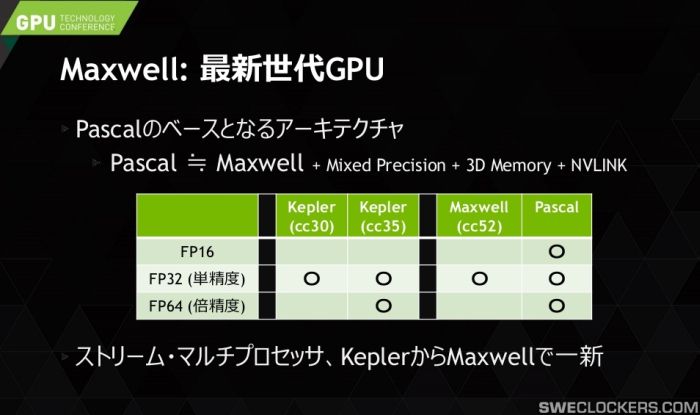
This basically proves that Pascal is Maxwell on 16nm + HBM2 + some compute stuff that was cut from Maxwell due to 28nm.
Wow. Maxwell was great and transforming into Pascal will make it even greater!
DX12 context switch great?Wow. Maxwell was great and transforming into Pascal will make it even greater!
This basically proves that Pascal is Maxwell on 16nm + HBM2 + some compute stuff that was cut from Maxwell due to 28nm.
So NVLINK is coming with Pascal as well. I assume if it's up there, it will appear in some high end motherboards.
That's when I'm building my 4k/60 PC.
EDIT: Actually, do they use the same chip names for their pro cards?
icecold1983
Member
if maxwell does turn out to be a poor performer in dx12, pascal unfortunately wont change it
This basically proves that Pascal is Maxwell on 16nm + HBM2 + some compute stuff that was cut from Maxwell due to 28nm.
Thus Volta is the real deal.
This basically proves that Pascal is Maxwell on 16nm + HBM2 + some compute stuff that was cut from Maxwell due to 28nm.
Will it be enough to be competitive with AMD's 400 series ?
if maxwell does turn out to be a poor performer in dx12, pascal unfortunately wont change it
Then we wouldn't see a major improvement until possibly Volta.
edit: beaten.
No idea if they chose Samsung 14nm or TSMC FF+. Also whether maintaining GCN is holding them back or not.Will it be enough to be competitive with AMD's 400 series ?
Chucke1992
Banned
DX12 context switch great?
Why should I care? End user does not know and care regarding how many calls is done inside GPU or whatever.
Whatever provides me with best experience - that will be my choice.
No idea if they chose Samsung 14nm or TSMC FF+. Also whether maintaining GCN is holding them back or not.
TSMC will manufacture their chips, not Samsung. Obviously we don't know much at all about the new rounds of GPUs but if async compute is going to be as big as some people claim then it's a bit short-sighted on Nvidia's part not to include something akin to AMD's ACEs. Or perhaps async compute can still be fully supported with their Pascal setup, no idea for now.
Oops sorry I meant AMD choosing a foundry.TSMC will manufacture their chips, not Samsung. Obviously we don't know much at all about the new rounds of GPUs but if async compute is going to be as big as some people claim then it's a bit short-sighted on Nvidia's part not to include something akin to AMD's ACEs. Or perhaps async compute can still be fully supported with their Pascal setup, no idea for now.
Nvidia has chosen TSMC 16FF+.
This is what happens when a node is skipped. Not that surprising really to be honest but I guess the date assumes no respins or other issues with the die, which on a new node using new tech feels a bit optimistic but still doable.
Being stuck with 28nm has really stagnated GPU performance so I am glad we they are finally moving on.
Being stuck with 28nm has really stagnated GPU performance so I am glad we they are finally moving on.
Also optimistic now that Samsung has a competing foundry and smartphone uptake slowed. Two years ago it felt like TSMC was the only viable foundry yet preferred mobile business.This is what happens when a node is skipped. Not that surprising really to be honest but I guess the date assumes no respins or other issues with the die, which on a new node using new tech feels a bit optimistic but still doable.
Being stuck with 28nm has really stagnated GPU performance so I am glad we they are finally moving on.
Finished? You mean that's not the current state of play?They will safely do that once they finished curbstomping AMD into bankruptcy.
Maxwell was a pretty significant performance enhancement considering it was still on 28nm. By all reports there's nothing to suggest Pascal is going to be revolutionary; just a shrunken down Maxwell.Being stuck with 28nm has really stagnated GPU performance so I am glad we they are finally moving on.
Thus Volta is the real deal.
Yeah, but presumably, Volta won't be out until like...2018.
You are obviously not following the most recent developments.Why should I care? End user does not know and care regarding how many calls is done inside GPU or whatever.
Whatever provides me with best experience - that will be my choice.
Maxwell was a pretty significant performance enhancement considering it was still on 28nm. By all reports there's nothing to suggest Pascal is going to be revolutionary; just a shrunken down Maxwell.
As good as Maxwell is the improvements are nothing compared to what a die shrink would have provided. Instead of a 7Tflop Titan X / 980Ti a 20nm Maxwell would likely have been a 10-11 Tflop Titan X / 980Ti which is a significant improvement. Along with the fact the increased transistor density would have enabled more ROPS/TMUs and other parts to have had their numbers boosted as well.