• Hey, guest user. Hope you're enjoying NeoGAF! Have you considered registering for an account? Come join us and add your take to the daily discourse.

Xbox One APU - Die Photo - Courtesy of Chipworks

tipoo

Banned
What exactly Im looking at here?

Something like this?

9Z26YnP.jpg


Insane to think about it.

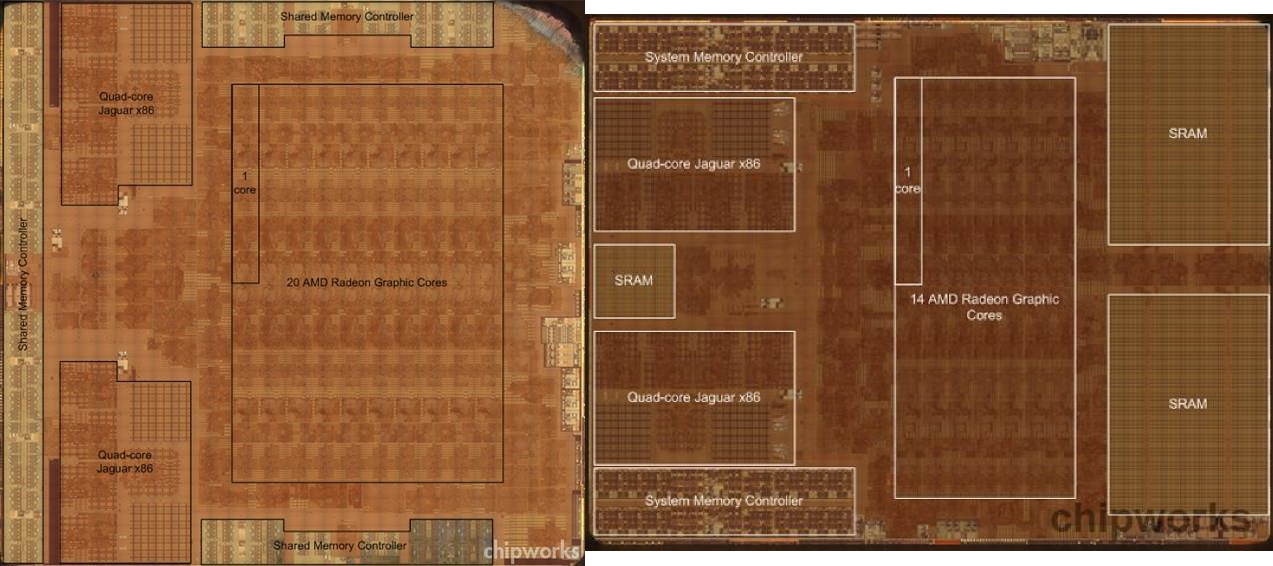
But in this case combined with the GPU and other subsystems. But yeah. You can see the die architecture exposed in your picture, what we have is just a better head-on scan of it.

I decapped CPUs and was able to see this stuff sometimes, it was so cool. SIM cards are a good way to see them, the chip is easy to see the architecture of (break apart the plastic and go for the tiny square in the middle, peel off some glue and you already see it)

Better shots of that Cell

45nm-cell-3.gif


386px-CeLL_die_large_qjpreviewth.jpg


You can see the memory blocks on that too, the square like stuff in each SPE.
 

Raist

Banned
What exactly Im looking at here?

Something like this?

9Z26YnP.jpg


Insane to think about it.

Something roughly half the size of a EU passport photo. Even smaller than that if you're from the US.

edit: I assume that pic is of the original 90nm Cell. Which was ~235mm^2. So these APUs are only 1.5x bigger.
 

onQ123

Member
I thought misterxmedia was just some clown website that didn't have many followers but then I see there's like hundred of comments waiting for the proof of this magic power boost to be proven now that xbox one is out.

Some people just need someone to believe in & sadly MisterXmedia is the hero that some sad X**ts ( I say that to separate the Xbox fans from these people because X**ts is the only way to describe these people they are not just Xbox fans ) needed & they will follow him to the end even years from now they will speak of the mystical Xbox One powers I even seen them asking him when he is going to make his own forum. They want a place where they can just lie to themselves about the Xbox One & PS4.


It's crazy!
 
Can I take a system with the die size of the Xbox but dedicated to GPU - looks like you could squeeze 28CUs on there, then the GDDR5 of the PS4?

Or better a system without an APU, that xbone die space dedicated to the gpu and a seperate intel cpu
For example an i5 2550k which is well over twice as fast as the ps4 cpu and clocks much higher only has a 1.16billion transistor die, which is less die space than is wasted on the esram for the xbone...

they used MORE than a gtx770 and an i5 2550k worth of transistor budget (on one single large die to add insult to injury) to end up with a cpu that is less than half as powerful and a gpu that is only a third as powerful and a hopeless memory bottleneck

Imagine if we had gotten subsidised consoles made for gaming first, and using a proper cpu and a nice gpu... maybe epic wouldn't have had to cancel their realtime GI for their engine and all those techdemos like luminous etc would have actually represented ingame graphics.
 

Tulerian

Member
Has anyone spotted the dGPU yet?

edit: why is there a small pool of SRAM on its own between the CPU cores?

The reason the Kinect gets so warm is the dGPU is in there, and is used to power the holographic emitters(disguised as IR emitters) to generate the holodeck in your living room.

Once you have been 'in' the new star trek game you'll see.
 

Proelite

Member
Or better a system without an APU, that xbone die space dedicated to the gpu and a seperate intel cpu
For example an i5 2550k which is well over twice as fast as the ps4 cpu and clocks much higher only has a 1.16billion transistor die, which is less die space than is wasted on the esram for the xbone...

they used MORE than a gtx770 and an i5 2550k worth of transistor budget (on one single large die to add insult to injury) to end up with a cpu that is less than half as powerful and a gpu that is only a third as powerful and a hopeless.

If you want a console that draws 250 watt and sound like a launch 360...
 

badb0y

Member
Some people just need someone to believe in & sadly MisterXmedia is the hero that some sad X**ts ( I say that to separate the Xbox fans from these people because X**ts is the only way to describe these people they are not just Xbox fans ) needed & they will follow him to the end even years from now they will speak of the mystical Xbox One powers I even seen them asking him when he is going to make his own forum. They want a place where they can just lie to themselves about the Xbox One & PS4.


It's crazy!

The saddest part about this whole misterxmedia thing is that Microsoft pretty much has laid out their APU and the GPU inside of it in the interview with Digital Foundry and they still refuse to except the truth.

In fact if you go read the blog right now they still don't believe in chip works photo.

Some gems I read:
"Xbox One die is darker that means it has more mass than PS4"

"No side X-ray? The Xbox One APU is stacked we are not seeing the full power!"

"The "secret sauce" is cloud computing. Forza 5 is the only game using it as of now and look at it. It's absolutely stunning and is running at 1080p 6fps! All because of the cloud."

Let them dream I guess.
 
Jesus, how poorly designed both chips are. One never gets used to those crappy automated designs AMD sells.

For reference, Haswell shot:

2.jpg


That minor orange area at the center-bottom is the only unused space of the whole chip.
 

CoG

Member
The saddest part about this whole misterxmedia thing is that Microsoft pretty much has laid out their APU and the GPU inside of it in the interview with Digital Foundry and they still refuse to except the truth.

Don't people realize that's just a windup site? Don't be trolled by misterxmedia.
 

Reg

Banned
Or better a system without an APU, that xbone die space dedicated to the gpu and a seperate intel cpu
For example an i5 2550k which is well over twice as fast as the ps4 cpu and clocks much higher only has a 1.16billion transistor die, which is less die space than is wasted on the esram for the xbone...

they used MORE than a gtx770 and an i5 2550k worth of transistor budget (on one single large die to add insult to injury) to end up with a cpu that is less than half as powerful and a gpu that is only a third as powerful and a hopeless memory bottleneck

Imagine if we had gotten subsidised consoles made for gaming first, and using a proper cpu and a nice gpu... maybe epic wouldn't have had to cancel their realtime GI for their engine and all those techdemos like luminous etc would have actually represented ingame graphics.

Just curious how much you would be willing to spend on such a device?
 

i-Lo

Member
Jesus, how poorly designed both chips are. One never gets used to those crappy automated designs AMD sells.

For reference, Haswell shot:

http://cdn3.wccftech.com/wp-content/uploads/2013/09/2.jpg[IMG]

That minor orange area at the center-bottom is the only unused space of the whole chip.[/QUOTE]

Damn, it's a shame that neither MS nor Sony were smart enough to know what they were buying into and modifying. If only they had contacted you for the PSA.
 

strata8

Member
Jesus, how poorly designed both chips are. One never gets used to those crappy automated designs AMD sells.

For reference, Haswell shot:

2.jpg


That minor orange area at the center-bottom is the only unused space of the whole chip.

I can't really see any unused space on the AMD chips that doesn't look intentional, given the consistent gaps between components. Maybe you can point them out?

Look at the Xbox One APU. Remove the gaps there and it fits together like a puzzle. Same deal with the PS4 apart from the spaces in the middle of the memory controller.
 
Damn, it's a shame that neither MS nor Sony were smart enough to know what they were buying into and modifying. If only they had contacted you for the PSA.

The only shameful thing here is both MS ans Sony going for AMD subpar designs.

Radeon cores look wonderful, though.

I can't really see any unused space on the AMD chips that doesn't look intentional, given the consistent gaps between components. Maybe you can point them out?

Look at the Xbox One APU. Remove the gaps there and it fits together like a puzzle. Same deal with the PS4 apart from the spaces in the middle of the memory controller.

No, they don't fit. Here is a read about how AMD design DIE area now:

http://www.xbitlabs.com/news/cpu/di...x_AMD_Engineer_Explains_Bulldozer_Fiasco.html

Another example of a good DIE design from IBM:

cell.jpg


For the price they're paying, I doubt they could have gotten anything better.

That's the problem, they went too cheap :/
 

badb0y

Member
The only shameful thing here is both MS ans Sony going for AMD subpar designs.

Radeon cores look wonderful, though.


No, they don't fit. Here is a read about how AMD design DIE area now:

http://www.xbitlabs.com/news/cpu/di...x_AMD_Engineer_Explains_Bulldozer_Fiasco.html

Another example of a good DIE design from IBM:

cell.jpg


That's the problem, they went too cheap :/

Yea they went cheap but did they really have a choice? Sony and Microsoft both lost money this generation and they certainly don't want to repeat that again.
 

wsippel

Banned
That's a good article, but it says nothing about unused space on the die. Automated designs are only used for the smaller logic components, not for the layout of the die as a whole.
Look at Latte. That's a billion transistor chip and it sure looks like it used an automated design for the whole layout, from the floor plan down to individual blocks, but at the same time, there's hardly any unused space. If that was done manually, somebody at AMD or Renesas has to be a huge fan of puzzles.
 

Nozem

Member
The saddest part about this whole misterxmedia thing is that Microsoft pretty much has laid out their APU and the GPU inside of it in the interview with Digital Foundry and they still refuse to except the truth.

In fact if you go read the blog right now they still don't believe in chip works photo.

Apparently Sony is paying Chipworks. Yeah.

lol
 

AlfeG

Member
Yes of course

- Chipworks is SDF for using fake/misleading x-ray shots
- Digital Foundry is SDF for saying BF4 looks better on PS4 and criticizing the short fallings of Forza
- "SonyGAF" is owned by Sony
- N4G is SDF because they only show pro-Sony articles and hide positive Xbone ones
- Sony is broke, but they have paid off all the journalists to say PS4 games look better


did i miss any?

Ha ha ha. Yes You miss.
Chipworks have photoshoped images =)
this xray is false.. I ask you all to wait a little longer... clearly more sony fud
SONY payed lies..
 

tipoo

Banned
Jesus, how poorly designed both chips are. One never gets used to those crappy automated designs AMD sells.

For reference, Haswell shot:


That minor orange area at the center-bottom is the only unused space of the whole chip.

*Rolls eyes*
How do you know what parts of the PS4 or XBO APU are wasted space? The shots can only provide an overview of larger structures, they can't show everything. And that Intel CPU shot you posted is a colorized shot, not a die scan, which would look more similar to the OP in terms of structures we can and can't see.

I grant you that the automated layout has disadvantages, but if you just look at what spots appear bare to your naked eye in one picture, that's silly and unrelated. The automated layout will have had to do with the micro side of the layout within the larger structures, not the macro which we can see. It's about the hundreds of millions of transistors we cant' see.
 

kitch9

Banned
Jesus, how poorly designed both chips are. One never gets used to those crappy automated designs AMD sells.

For reference, Haswell shot:

2.jpg


That minor orange area at the center-bottom is the only unused space of the whole chip.

Instead of regurgitating any vague bullshit you find on the net maybe you should get at least a tiny bit of knowledge about the subject in hand.
 

Perkel

Banned
The only shameful thing here is both MS ans Sony going for AMD subpar designs.

Radeon cores look wonderful, though.

No, they don't fit. Here is a read about how AMD design DIE area now:
Another example of a good DIE design from IBM:


That's the problem, they went too cheap :/


Honestly who gives a shit how much real space actual hardware take on chip ? Price matters and both IBM and Intel couldn't deliver worthwhile APU. What it matters in the end is price to performance ratio not how it looks.
 

onQ123

Member
Ha ha ha. Yes You miss.
Chipworks have photoshoped images =)


Insider Daily. Chipworks pictures are "strange"
November 27th, 11:57

Misterx: X-ray is out...where is side images. where is 2.5D tech?

Insider: Dont believe chipworks.. wait for team x to show there xrays and others... the chipworks xray have been ultred .. look at the original xray and then look at there diagram. They have marked and changed the number of cu' 14.. nope there is 18... they have also changed one block of sram which is actually the part of the 50mc units. There is only one cluster of sram and one memory controller for sram on final design. The data move engines are were the sram sit between the cpus.. this xray is false.. I ask you all to wait a little longer... clearly more sony fud. But expect others to speak out soon. I would believe this will be the straw that brakes the guys at redmond rnd.. sony has really crossed the line now.. the guys that put the x1 soc together ant happy and people are hearing this loud and clear.

Misterx: I see no xray for xb1 soc. Is it here? I see only microscoped first metal layer in yellow-toned image...Xray would look monocromic(gray and white only colors)...Is xray image look like this or it is microscoped?

Insider: The pictures chipworks have up loaded are the top layer of the main soc.. they are drawing there own conclusion as to how big the gpu is.. and sram.. they have even changed the diagram to mirror the vgleaks .. they even use the same analogy as many as favor towards ps4 architecture. SONY payed lies.. even tho the gpu part is dp.. it has 16cu that can be used but 2 more that can not be accessed 18cu. But 14cu are available but two are reserved for kinect these can be used for games, as kinect has its own processors. But kinect can off load to these cu if need be.... they dont even go into detail of the packaging of the transistor budget. And the really annoying party is they cant figure out wii u part but they rule out the diagram to x1 based on leaks.. The real reason these fudging of the numbers and truth are happening about faults and other things is because ms wont pay these websight cash. And sony does half of gaf / n4g are payed by a corporate body of sony. Ms should open the flood gates at vgx then come back and keep looking at these diagrams and ask your self how. Nobody wants to see sony fall. But ms need and must stand by there console and design. There rnd department are not happy. But others are going to show xrays soon not the best of sight to find out from but adlest they dont post fud. Also please get mister c to go over the soc .. he will see that it dont add up ..

MIsterx: Are thouse pictures Xrays or microscoped 1st layer?

Insider: Microscope first layer.. dark silicon is or can be multi lay.. chip stacking means chips can be stacked does not have to be whole layer.. the xray will tell a different story but it will look strange with the transistor packaging. Chipworks have taken the microsocpe and drawn there own conclusion that is a direct copy of the vgleaks which are wrong. You can tell the cu budget has been changed .. there is a lot of errors


GoodGrief-703274.gif


LOL
 

Binabik15

Member
As long as nobody (but one or two brave messengers to get the quotes) gives him clicks I see no harm in GAF laughing at his antics.

He's like some of the Wii U believers, but with worse spelling and probably a joke character.
 

Cuth

Member
Yea they went cheap but did they really have a choice? Sony and Microsoft both lost money this generation and they certainly don't want to repeat that again.
I don't think MS would've lost money without the RROD problem, something they obviously worked to avoid this time. Wanting to make money from the hardware even at launch is a sign of pure greediness.

But the hardware it's not the whole picture at all. Compared to 10 years ago the situation from the gamers is something like this:
- worse deal on the hardware
- forced to pay to play online and use some services
- ads thrown around in UI and games
- gathering of valuable consumer information

And, I'm sure, the console makers still asks for royalties for every copy of third parties' games (or an hefty percentage for the digital sales). They should drop this completely and push the publishers to reduce the selling price of the games, given how may other ways they have to make money from their customers.
It's like they're using the "razor and blades business model" without the reduction of the entry price for the customers that is a fundamental part of it.
 
*Rolls eyes*
How do you know what parts of the PS4 or XBO APU are wasted space? The shots can only provide an overview of larger structures, they can't show everything. And that Intel CPU shot you posted is a colorized shot, not a die scan, which would look more similar to the OP in terms of structures we can and can't see.

I grant you that the automated layout has disadvantages, but if you just look at what spots appear bare to your naked eye in one picture, that's silly and unrelated. The automated layout will have had to do with the micro side of the layout within the larger structures, not the macro which we can see. It's about the hundreds of millions of transistors we cant' see.

It's not difficult at all to spot unused silicon on a die shot like this. And, of course, I'm not doing anything using my naked eye, that is an image with an high magnification. Those guys reverse engineer chips using images like this one and more detailed. They just not release them to public without a fee usually.

Chipworks have helped emulation communities in the past giving away die shots of older chips, so coders were be able to figure undocumented stuff. It isn't an obscure magic trick.

Instead of regurgitating any vague bullshit you find on the net maybe you should get at least a tiny bit of knowledge about the subject in hand.

Many thanks for your insightful input.

Honestly who gives a shit how much real space actual hardware take on chip ? Price matters and both IBM and Intel couldn't deliver worthwhile APU. What it matters in the end is price to performance ratio not how it looks.

But unused area cost money, lowers performance and raise power leaks.

We already knew that CPU were 2 quad cores 'glued' together. Not being monolithic leads to that waste of silicon between both modules. Also means worse data sharing between them, since they don't share the same pool of L2 and must use and external interface.

Dunno, I think a thread like this is the right place to discuss this stuff. I'm sorry if anyone got offended by any criticism regarding some aspect of their platform of choice.
 

Astroroot

Banned
At the end of the day Cerny and Sony took a gamble and won. This same gamble could have easily rendered them with a console with half the total memory of Xbox One.

Both consoles had the same budget (BoM, TDP, calendar) and had to allocate resources within these restraints. This is pretty much confirmation that eSRAM, not Kinect is the main reason for the power differential. Even with 24 CUs the console would still cost $100 more with Kinect.

What perplexes me is why didn't MS just go with an eSRAM daughter die and rely on die shrinks down the road? On top of that, the only reason Xbox One has 8 GB of memory is due to Hyper-V. If this was just an evolution of the X360 OS, MS would have launched with 4 GB of GDDR5 and a faster GPU.
 

onQ123

Member
At the end of the day Cerny and Sony took a gamble and won. This same gamble could have easily rendered them with a console with half the total memory of Xbox One.

Both consoles had the same budget (BoM, TDP, calendar) and had to allocate resources within these restraints. This is pretty much confirmation that eSRAM, not Kinect is the main reason for the power differential. Even with 24 CUs the console would still cost $100 more with Kinect.

What perplexes me is why didn't MS just go with an eSRAM daughter die and rely on die shrinks down the road? On top of that, the only reason Xbox One has 8 GB of memory is due to Hyper-V. If this was just an evolution of the X360 OS, MS would have launched with 4 GB of GDDR5 and a faster GPU.

More like DDR3 is the reason.
 

Nerfon

Member
Not only the esram but also half rops are xbox one weakness.
Esram use will get better but no code can restore 16 missing rops and the caches on the rops.
 

tipoo

Banned
It's not difficult at all to spot unused silicon on a die shot like this. And, of course, I'm not doing anything using my naked eye, that is an image with an high magnification. Those guys reverse engineer chips using images like this one and more detailed. They just not release them to public without a fee usually.

Chipworks have helped emulation communities in the past giving away die shots of older chips, so coders were be able to figure undocumented stuff. It isn't an obscure magic trick.

You skipped an important point. The Haswell die you pointed to with less wasted space to your eye, is a colorized representation. Actual scans show similar empty areas littered through.
 

strata8

Member
But unused area cost money, lowers performance and raise power leaks.

Compared to what?

- $100 chip cost
- 348mm2 die size
- Total system power consumption of 140W, so APU TDP likely under 120W
- CPU performance equal to an i3-3220
- GPU performance between a 7850 and 7870

Since you called the design "shitty", could someone else have done significantly better with the same cost, size, and power constraints?
 
Top Bottom