I'd love to think that the bus is 128bit, but... the Shield TV also has 2 mem chips, in the exact same configuration, so whatever the Sheild TV is, I think it's a high probability that this thing is too.Which is why I think the 64bit bus is fine for memory, the issue I have is 2 chips being an odd decision for final hardware but not matter much in a prototype of a limited run.
IE, 2 chips would suggest 128bit memory bus, though a July devkit would use 64bit.
-
Hey, guest user. Hope you're enjoying NeoGAF! Have you considered registering for an account? Come join us and add your take to the daily discourse.
You are using an out of date browser. It may not display this or other websites correctly.
You should upgrade or use an alternative browser.
You should upgrade or use an alternative browser.
A Nintendo Switch has been taken apart
- Thread starter Dystify
- Start date
Schnozberry
Member
Both the layout of all the passives on the package and the die size appear to be an exact match. That's not something I'd expect to just happen with radically different SoCs.
Yeah, I'm with Durante on this one. I think we're most likely looking at a lightly modified X1. They may have tinkered with the caches or (if you're willing to be pie in the sky) shrunk the design down to 16nm for power efficiency, but the dies are too close in size to expect any radical departures.
Final clock speeds and hopefully microscopic analysis at some point will be fun to peek at.
LordOfChaos
Member
Yeah, I'm with Durante on this one. I think we're most likely looking at a lightly modified X1. They may have tinkered with the caches or (if you're willing to be pie in the sky) shrunk the design down to 16nm for power efficiency, but the dies are too close in size to expect any radical departures.
Final clock speeds and hopefully microscopic analysis at some point will be fun to peek at.
Thirded. That the die size is almost an exact match to the TX1, if they did all these crazy modifications and moved to a different node? Ehh. If it acts like a duck...
Not that it would be 100% TX1, but it'll be much closer to it than previous efforts like Espresso/Latte. It will be interesting to see if Nintendo touched the memory chain, which they've agonized over since the blunder with the N64.
A big piece of this is the bend Nvidia was in with wafer silicon agreements from the Tegra team. They tried the Shields to move some silicon, didn't sell great...I think Nintendo potentially found a windfall here with minor mods to the TX1 and buying out the remaining orders.
With the photos of the board in this thread being so dated (FCC approval switch or early prototype)
There's so much right with Foxconn leaks so far that i don't think we can put that benchmark leak under the rugs..
I'm in team believe @ 512 cuda cores
thisisneogaf.gif
I don't care if it does not happen, i'm fine with just a TX1. But... "what if"..
Foxconn leak is 100% not 512 cuda cores, it leaks the size of the SoC to be around 100mm, 512 cuda cores would mean around 50% bigger chip. It's 256 cuda cores and 4 CPU cores of a various clock. The foxconn clocks were tested, and best explanation for that is that it is being used in retail devices, but no foxconn leak isn't some magical super device.
Schnozberry
Member
Thirded. That the die size is almost an exact match to the TX1, if they did all these crazy modifications and moved to a different node? Ehh. If it acts like a duck...
Not that it would be 100% TX1, but it'll be much closer to it than previous efforts like Espresso/Latte. It will be interesting to see if Nintendo touched the memory chain, which they've agonized over since the blunder with the N64.
A big piece of this is the bend Nvidia was in with wafer silicon agreements from the Tegra team. They tried the Shields to move some silicon, didn't sell great...I think Nintendo potentially found a windfall here with minor mods to the TX1 and buying out the remaining orders.
Nintendo will sell more Switches in the first month than Nvidia has sold for all the Shield devices combined lifetime to date. It's a huge win for the Tegra Team and it will definitely keep Nvidia invested with furthering low power tech.
UnemployedVillain
Member
A big piece of this is the bend Nvidia was in with wafer silicon agreements from the Tegra team. They tried the Shields to move some silicon, didn't sell great...I think Nintendo potentially found a windfall here with minor mods to the TX1 and buying out the remaining orders.
This nonsense again? Nintendo didn't just buy leftover Tegra chips. It's a ridiculous assertion to make.
20nm and 16nm chips are about the same size, so no what we see gives us no indication of the nature of the chip, in the end a 20nm X1 chip shouldn't be possible at Foxconn clocks for 8 days straight with that meager cooling solution without throttling, but there was no frame drops.
We can write that off as some odd ball test they did to prove nothing at all, you know because they want to do that for 8 days. No the clocks were useful for something, we just don't know what that is yet.
As for LCGeek, that bench mentioned, LCGeek only knew about 4 cores, never mentioned 1 being unusable for games (though this could always change as they move to final software and get everything working right)
1100 x 6.5 = 7150
1800 x 4 = 7200
This single threaded benchmark does not actually work like this and it is also worth noting that single threaded performance is more important than multicore performance as long as you have 3 cores, so it is likely pretty easy to move code to the Switch* from the PS4, as logic just runs faster, and the overall throughput is going to have light bottlenecks at worse.
*Big issue here is we just don't know that Nintendo went with these clocks or A72, but we aren't long away from having the device in our own hands and someone among "us" will dive a bit deeper and answer these questions.
Well, it really depends on the size of the floorplan and the points they're monitoring. Approaching 10C of delta is achievable on the some dies, if they monitored t-junction at sufficiently remote locations. Now, whether they could load _all_ CPU cores, along with the GPU (and thus saturate the thermal map), and still get large differences is really up to the peculiarities of the specific floorplan. For instance, IIRC, I can get deltas of ~7C across certain cores on my Xeon without much issue, but that's at largely asymmetrical loads and at 22nm a xeon is not a small die.
A fair point, and I can imagine for a large Xeon die (particularly with only one core active) there may be a larger difference in temps, but it seems a bit of a stretch for a ~120mm² die like this, especially when you would expect a large portion of the silicon to be in use. I'd also expect the largest deltas under load, whereas here we're supposedly seeing a 14 degree difference while idle.
Right, clusterization can go in pairs as well, but it's traditionally done for binning purposes - when you have a SKU of 2 cores and a SKU of 4 cores, and you want to bin the smaller from the larger. I can't see such a use case for nintendo.
Yeah, it doesn't make much sense for Nintendo. I can't really think of other situations where it makes sense, though. If this is a benchmark of something (as opposed to someone just plucking numbers off the top of their head), then what chip would have that kind of odd clocking arrangement? Is it possible that the clock speed switching is sufficiently rapid that the clocks actually changed between readouts for each core?
Thor is the Norse god of war. Odin is the god of wisdom. So it's a wise choice by Nintendo.
Ah, thanks for the clarification. I'm clearly going to have to study up on Norse mythology if I'm to decipher the secret of the Switch.
There is no way in hell that the Switch will have UHS II support in speed even if it can access it, the pins are not the same. They would not shell out the money for it, at least not the first edition ones, maybe, and that's a big maybe, they will have it in later revisions or a Nintendo NEW(xN) Switch.
There are extra pins, but it's compatible with regular microSD (i.e. you can use a regular microSD in a UHS-II slot, and a UHS-II microSD in a regular microSD slot). As I've said though, I think it's extremely unlikely, but the photos we've got don't give us any confirmation one way or the other (removing the metal shield would allow us to see if the UHS-II pins are there).
Yeah, I'm with Durante on this one. I think we're most likely looking at a lightly modified X1. They may have tinkered with the caches or (if you're willing to be pie in the sky) shrunk the design down to 16nm for power efficiency, but the dies are too close in size to expect any radical departures.
Final clock speeds and hopefully microscopic analysis at some point will be fun to peek at.
The other possibility is that the new Shield TV uses Switch's SoC, rather than the other way around. The 2017 Shield TV does have a revised SoC, with visibly different chips and a change from model number TM670D-A1 to TM670M-A2, and Nvidia have in the past often used the same Tegra chip name for multiple variants (most notably the K1 with A15 cores and the other K1 with Denver cores). The commonality for Tegra chips of a given name seems to be their GPU configuration, with the two K1s both having 192-core Kepler GPUs, but vastly different CPUs. On Nvidia's page for the new Shield TV you'll see a much simpler description of the Tegra X1 than they gave before:
NVIDIA® Tegra® X1 processor with a 256-core GPU and 3 GB RAM
There's no mention of the CPU at all here. As with the variants of the K1, there may be changes outside the GPU config which they don't feel warrant a new code. Unlike the K1, though, these changes may not have been driven by Nvidia's internal requirements, but rather by Nintendo's. Nintendo may have requested customisations such as a change in CPU config, a different manufacturing process, or perhaps just some low-level tweaks here and there, and Nvidia may have decided it was simpler to just brand the new chip as Tegra X1 for use in their own device, rather than continue manufacturing two separate chips. This would be particularly true if they were moving to 16nm, as I'm sure Nvidia would be eager to leave 20nm behind.
The one issue I have with such a theory, though, is it would mean Switch's SoC still has the full 4K h.265 encode/decode functionality, which is pretty much the first thing I would have imagined Nintendo getting rid of were they to customise the TX1.
Edit: Although, I suppose it's possible that they actually dropped the 4K h.265 encoding, as the Shield TV doesn't make use of it, afaik. Decode likely takes up less die space.
UnemployedVillain
Member
The one issue I have with such a theory, though, is it would mean Switch's SoC still has the full 4K h.265 encode/decode functionality, which is pretty much the first thing I would have imagined Nintendo getting rid of were they to customise the TX1.
.
Why? Wouldn't they need it if they ever planned on supporting 4K video, such as when video apps like Netflix, Hulu, Amazon Prime, etc come along?
Why? Wouldn't they need it if they ever planned on supporting 4K video, such as when video apps like Netflix, Hulu, Amazon Prime, etc come along?
Encoder, I doubt the switch would encode your gaming at 4k, so there is no point in keeping it.
UnemployedVillain
Member
Encoder, I doubt the switch would encode your gaming at 4k, so there is no point in keeping it.
Well he clumped encode/decode. I guess it would only need the decoder, but if that's there, why bother even going through the effort of removing the encoder?
Well he clumped encode/decode. I guess it would only need the decoder, but if that's there, why bother even going through the effort of removing the encoder?
Iirc switch officially only supports 1080p output from the dock, which is fine, since they could always release a 4k dock with its own gpu for 4k gaming and video in the future. HD burned Nintendo so it's something they might do.
The other possibility is that the new Shield TV uses Switch's SoC, rather than the other way around. The 2017 Shield TV does have a revised SoC, with visibly different chips and a change from model number TM670D-A1 to TM670M-A2, and Nvidia have in the past often used the same Tegra chip name for multiple variants (most notably the K1 with A15 cores and the other K1 with Denver cores). The commonality for Tegra chips of a given name seems to be their GPU configuration, with the two K1s both having 192-core Kepler GPUs, but vastly different CPUs. On Nvidia's page for the new Shield TV you'll see a much simpler description of the Tegra X1 than they gave before:
There's no mention of the CPU at all here. As with the variants of the K1, there may be changes outside the GPU config which they don't feel warrant a new code. Unlike the K1, though, these changes may not have been driven by Nvidia's internal requirements, but rather by Nintendo's. Nintendo may have requested customisations such as a change in CPU config, a different manufacturing process, or perhaps just some low-level tweaks here and there, and Nvidia may have decided it was simpler to just brand the new chip as Tegra X1 for use in their own device, rather than continue manufacturing two separate chips. This would be particularly true if they were moving to 16nm, as I'm sure Nvidia would be eager to leave 20nm behind.
The one issue I have with such a theory, though, is it would mean Switch's SoC still has the full 4K h.265 encode/decode functionality, which is pretty much the first thing I would have imagined Nintendo getting rid of were they to customise the TX1.
Edit: Although, I suppose it's possible that they actually dropped the 4K h.265 encoding, as the Shield TV doesn't make use of it, afaik. Decode likely takes up less die space.
So if the new Shield uses A72s at 16nm, wouldn't that be easily visible in benchmarks?
Real of fake? You decide:
Where does this "leak" claim to come from? Is it also saying it's from foxconne or is it supposed to be a benchmark from somewhere else? Any speakers of chinese see anything reguarding this?
LordOfChaos
Member
This nonsense again? Nintendo didn't just buy leftover Tegra chips. It's a ridiculous assertion to make.
It's also not the one I made, the only nonsense is not understanding what I said.
They had to buy a number of chips per their wafer silicon agreement, the Nintendo deal was probably well timed for the predicament Nvidia was in or they'd be hit by large fines anyways. The Switch SoC is most likely very TX1-like, but I'm not saying they bought a bunch of leftover chips in a warehouse. It's customized, and new chip orders, but it still fills the WSA
Nintendo will sell more Switches in the first month than Nvidia has sold for all the Shield devices combined lifetime to date. It's a huge win for the Tegra Team and it will definitely keep Nvidia invested with furthering low power tech.
Exactly. Purportedly the Tegra team was also told to get a large design win or go home, it's still important for PX Drive but maybe risked being its own department anymore.
Iirc switch officially only supports 1080p output from the dock, which is fine, since they could always release a 4k dock with its own gpu for 4k gaming and video in the future. HD burned Nintendo so it's something they might do.
Is this actually true? How would the 4k dock interface with the Switch? It only has that one USB port right?
Where does this "leak" claim to come from? Is it also saying it's from foxconne or is it supposed to be a benchmark from somewhere else? Any speakers of chinese see anything reguarding this?
Whatever that is a benchmark of, its not the Switch. Its universally debunked by techgaf
")
Why? Wouldn't they need it if they ever planned on supporting 4K video, such as when video apps like Netflix, Hulu, Amazon Prime, etc come along?
Well it doesn't seem to be much of a priority for them, especially as they don't have any video services available at launch. That's not to say I don't expect Netflix, etc., to appear down the line, just that it's clearly not something Nintendo's focussing on with Switch.
Effectively it's all a matter of rationing die space, and if Nintendo were to have the option of allocating a given amount of die area to supporting 4K Netflix, or allocating it to gaming-related hardware, I would assume they'd choose the latter (or just take a smaller, cheaper die).
Buggy Loop
Member
Where does this "leak" claim to come from? Is it also saying it's from foxconne or is it supposed to be a benchmark from somewhere else? Any speakers of chinese see anything reguarding this?
It's from here
You can check around the images, there's conversations too.
Translation though?? That's another problem.
UnemployedVillain
Member
It's also not the one I made, the only nonsense is not reading what I said.
They had to buy a number of chips per their wafer silicon agreement, the Nintendo deal was probably well timed for the predicament Nvidia was in or they'd be hit by large fines anyways. The Switch SoC is most likely very TX1-like, but I'm not saying they bought a bunch of leftover chips in a warehouse. It's customized, and new chip orders, but it still fills the WSA
Exactly. Purportedly the Tegra team was also told to get a large design win or go home, it's still important for PX Drive but maybe risked being its own department anymore.
They're already releasing a new Shield using those same chips, so what "predicament" were they in?
Here is a question. Miyamoto said they knew they messed up with Wii U's CPU. He said they would fix this mistake next go round (Switch). How does using 3 underclocked A57's help? Is it that much better a solution then what Wii U had compared to XB1 and PS4?
What are you talking about?
So if the new Shield uses A72s at 16nm, wouldn't that be easily visible in benchmarks?
I wouldn't necessarily expect either, but if they were still using A57s, but jumped down to 16nm, then you may see an improvement in performance on the new Shield, just from reduced throttling.
It's from here
You can check around the images, there's conversations too.
Translation though?? That's another problem.
A translation was posted a few pages back by dahuman.
LordOfChaos
Member
They're already releasing a new Shield using those same chips, so what "predicament" were they in?
And how many units do you recon the Shield TV will launch vs the Switch? What part is causing you confusion? Nvidia was unhappy with TSMC 20nm, but had a contractual obligation to by x millions of chips. The Shield attempts to move some, but the Switch will probably outdo all combined Shield sales in months if not one month.
https://www.extremetech.com/computi...y-with-tsmc-claims-22nm-essentially-worthless
So if Nintendo came along asking about some chips, they may have gotten quite the steal just so Nvidia could avoid contractual break fees. Not old chips in a warehouse, that's of course ridiculous, but new orders that filled the 20nm contract.
UnemployedVillain
Member
And how many units do you recon the Shield TV will launch vs the Switch? What part is causing you confusion? Nvidia was unhappy with TSMC 20nm, but had a contractual obligation to by x millions of chips. The Shield attempts to move some, but the Switch will probably outdo all combined Shield sales in months if not one month.
https://www.extremetech.com/computi...y-with-tsmc-claims-22nm-essentially-worthless
So if Nintendo came along asking about some chips, they may have gotten quite the steal just so Nvidia could avoid contractual break fees. Not old chips in a warehouse, that's of course ridiculous, but new orders that filled the 20nm contract.
Okay, this makes more sense. Thanks for the clarification
blu
Wants the largest console games publisher to avoid Nintendo's platforms.
Actually that's one possibility.Yeah, it doesn't make much sense for Nintendo. I can't really think of other situations where it makes sense, though. If this is a benchmark of something (as opposed to someone just plucking numbers off the top of their head), then what chip would have that kind of odd clocking arrangement? Is it possible that the clock speed switching is sufficiently rapid that the clocks actually changed between readouts for each core?
There are extra pins, but it's compatible with regular microSD (i.e. you can use a regular microSD in a UHS-II slot, and a UHS-II microSD in a regular microSD slot). As I've said though, I think it's extremely unlikely, but the photos we've got don't give us any confirmation one way or the other (removing the metal shield would allow us to see if the UHS-II pins are there).
You said exactly what I said outside of the part where I refuse to believe it will be there when I unbox my Switch lol
There is just noway.Osiris
I permanently banned my 6 year old daughter from using the PS4 for mistakenly sending grief reports as it's too hard to watch or talk to her
So the benchmark puts the Switch close to xbox one in performance?
No. - Last reported clocks put it around 393 Gflops when docked, or about 40% of the power of an Xbox One.
It's from here
You can check around the images, there's conversations too.
Translation though?? That's another problem.
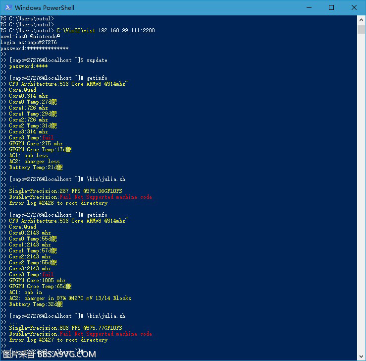
Thanks. It's interesting, just wish it had more context to it (maybe it does, just don't know chinese) so we can get a clearer picture of what's being claimed here, it just seemed to have been dropped on here out of the blue. I guess (if this was real) they'd do that Julia benchmark at 480x360 specifically to stress test the CPU?
i think some people are wrongfully taking the NX02 chip designation as meaning tegra X-2
some even spouting volta levels of cuda cores.
i think we need to be realistic here. this thing is faster than an tegra x-1, but its nowhere near the purported levels of volta or possibly even parker which is pascal based.
some even spouting volta levels of cuda cores.
i think we need to be realistic here. this thing is faster than an tegra x-1, but its nowhere near the purported levels of volta or possibly even parker which is pascal based.
UnemployedVillain
Member
i think some people are wrongfully taking the NX02 chip designation as meaning tegra X-2
some even spouting volta levels of cuda cores.
i think we need to be realistic here. this thing is faster than an tegra x-1, but its nowhere near the purported levels of volta or possibly even parker which is pascal based.
I don't think anyone is doing that, but going by their naming convention it's the second version of their NX customized chip
No. - Last reported clocks put it around 393 Gflops when docked, or about 40% of the power of an Xbox One.
He said the benchmark, not reported clocks though. Not that I believe that benchmark, seems odd.
LordOfChaos
Member
Here is a question. Miyamoto said they knew they messed up with Wii U's CPU. He said they would fix this mistake next go round (Switch). How does using 3 underclocked A57's help? Is it that much better a solution then what Wii U had compared to XB1 and PS4?
Significantly better, actually. Especially considering it's still in the market at the same time as the XBO and PS4, same as the Wii U. But, that's as much a testament to how much of a letdown it was that the Wii U used three PowerPC 750s (with only the gamecube modifications to the core logic, and multiprocessor/more cache/higher clock being the other tweaks).

That said, significantly better may not be what some had hoped. 20nm was a pretty poopy fabrication node, so I really do think Nintendo cashed in on Nvidia not being able to fulfil contractual order sizes on 20nm. Had it been 16nm, Cortex A72 would have been taped out on that and it would have made sense to use. Or even without that, updating the CCI to allow the OS to run on A53s while all A57s worked on the game would have been nice and freed up an extra 33% more game cores.
No. - Last reported clocks put it around 393 Gflops when docked, or about 40% of the power of an Xbox One.
Was talking more about the latest benchmark leak. I dont believe those clocks are accurate anymore because it doesnt march up with the data at hand.
Is this actually true? How would the 4k dock interface with the Switch? It only has that one USB port right?
Wouldn't be worth it, and depending on the HDMI version, the dock can already do 4K since I doubt it's older than HDMI 1.4. We don't even know the actual bandwidth of the USB-C on the Switch. If it's USB3.1 then I guess you can still do 4K 24FPS@ 8bits with videos fine, but if you want anything higher, you'd need either Thunderbolt or multiple PCIe lanes, and at least HDMI 2.0, which well, uh, I'm sure the Switch is missing at least 2 of those things.
Thanks. It's interesting, just wish it had more context to it (maybe it does, just don't know chinese) so we can get a clearer picture of what's being claimed here, it just seemed to have been dropped on here out of the blue. I guess (if this was real) they'd do that Julia benchmark at 480x360 specifically to stress test the CPU?
Nope, that's pretty much it, nothing more lol.
Actually I got more confused now.This may shed more light.
The pics you posted (assuming I got them right) sport a clustered config with A57s and A53s, and a HMP one with A17... yet, you said only newer ARM have proper big.LITTLE stuff, so I thought that would mean right the ones found in the Tegra X1.
Am I missing something, or even totally misunderstood the pics?
Genuine question, I have an IT background and I'd like to get a grasp on this (fascinating) stuff if possibile.
eighty(one)
Member
The timeline is fine. Here is the logic with what he is suggestion. He is saying that they sent out devkits at the same time new chips were being produced and then sat on those for 3+ months.
There is no reason they wouldn't just wait a few extra days to get the new chips in these devkits. It still being July Devkits, just means it doesn't take as long as he is thinking to ship these to developers, I mean if the chips are done on the 18th and foxconn is making the devkit (or even Nintendo given this is a prototype, and foxconn leak confirmed that at least 1 switch was put together internally at Nintendo)
This isn't the first devkit so Foxconn could put the chips on the devkit in a single day, possibly 2 and ship them to Nintendo well before the end of july to be shipped out to developers. Nintendo not using these chips for developers make no sense.
No the X1 chip was custom even then, just think about it, this is Revision #2, there was an A0 and A1, so they would all be custom Maxwell GPUs based on X1.
I also think we need to look at the foxcon leak and and disemminate when manufacture for retail HAD to begin. I remember reading they can make 20,000 per day. If they started in October and went through all of Feb at 30 days X 20,000 = 2.4 million. However, we need to be aware February likely is a wash, since these units are already in process to retail for 3/3 launch.
Remember, Kimishima expected only 2 million for launch.
I'm thinking this unit was likely in the test batch or retail manufacture run - if so, it's likely close to final.
LordOfChaos
Member
Actually I got more confused now.
The pics you posted (assuming I got them right) sport a clustered config with A57s and A53s, and a HMP one with A17... yet, you said only newer ARM have proper big.LITTLE stuff, so I thought that would mean right the ones found in the Tegra X1.
Am I missing something, or even totally misunderstood the pics?
Genuine question, I have an IT background and I'd like to get a grasp on this (fascinating) stuff if possibile.
It's to do with the connection, not the ARM core type. Tegra X1 used the first version of big.little, you can have the high performance cluster on, or the low performance, period. If any task pegged any one of the little cores, all tasks would switch to the big cores, it was pretty 'dumb'.
Version 2 is within each high/low core pair, you can have either on, i.e 2 little 2 big, all big, 1 big 3 little, etc, on at once. But for a 4+4 arrangement, never more than 4 cores on at once still.
Verson 3, HMP, is that you can seamlessly interleave core types. This is what you'd need to run the Switch OS on a little core while running the big ones all for the game, as you could have all the little and all the big on at the same time, or 1 little, 4 big, or any combination thereof, and it's all controlled by the kernel.
mario_O
Member
Here is a question. Miyamoto said they knew they messed up with Wii U's CPU. He said they would fix this mistake next go round (Switch). How does using 3 underclocked A57's help? Is it that much better a solution then what Wii U had compared to XB1 and PS4?
If the Eurogamer leak is true: 3 cores @1Ghz, in both docked and hanheld, it looks really weak indeed.
I also think we need to look at the foxcon leak and and disemminate when manufacture for retail HAD to begin. I remember reading they can make 20,000 per day. If they started in October and went through all of Feb at 30 days X 20,000 = 2.4 million. However, we need to be aware February likely is a wash, since these units are already in process to retail for 3/3 launch.
Remember, Kimishima expected only 2 million for launch.
I'm thinking this unit was likely in the test batch or retail manufacture run - if so, it's likely close to final.
Don't forget Chinese New Year month where they pretty much don't do shit when it comes to manufacturing.
LordOfChaos
Member
If the Eurogamer leak is true: 3 cores @1Ghz, in both docked and hanheld, it looks really weak indeed.
exactly!
Miyamoto said that and then stepped down from having input on the hardware specs so...Heh. I hope the next guys didn't miss the memo.
But, 3 Cortex A57s are still >>>> 3 PowerPC 750s
fluffydelusions
Member
I'm assuming the battery being from the galaxy note 7 supplier has already been talked about?
http://nintendotoday.com/nintendo-switch-battery/
http://nintendotoday.com/nintendo-switch-battery/
Miyamoto said that and then stepped down from having input on the hardware specs so...Heh. I hope the next guys didn't miss the memo.
But, 3 Cortex A57s are still >>>> 3 PowerPC 750s
I remember investors actually asking Iwata if the cpu was underpowered. I don't think Nintendo forgot.
UnemployedVillain
Member
I'm assuming the battery being from the galaxy note 7 supplier has already been talked about?
http://nintendotoday.com/nintendo-switch-battery/
There's literally a whole thread about it
Oh... so basically you *could* build a Tegra X1 where the A53s were running the OS by including the appropriate big.little tech?It's to do with the connection, not the ARM core type. Tegra X1 used the first version of big.little
For some reason I thought big.little was exclusively available on certain, mostly recent ARM cores, hence my confusion.
Thanks for the explaination (that is, assuming I got it right this time)
BRocknRolla
Member
There's literally a whole thread about it
And I'm still unclear why that existed as well.
LordOfChaos
Member
Oh... so basically you *could* build a Tegra X1 where the A53s were running the OS by including the appropriate big.little tech?
For some reason I thought big.little was exclusively available on certain, mostly recent ARM cores, hence my confusion.
Thanks for the explaination (that is, assuming I got it right this time)
Yup you got it, you can technically update most modernish ARM designs with the new connective fabric. Hence Tegra X1, which has ARM cores that already have HMP in other designs, not having it, and having the primitive first generation whole cluster switching.
Not sure where the cutoff point is for ARM core compatibility, I think there is one, but the big.LITTLE version isn't tied to core types.
Similar threads
- 70
- 7K
Deerock71
replied
- Locked
- 12
- 2K