-
Hey, guest user. Hope you're enjoying NeoGAF! Have you considered registering for an account? Come join us and add your take to the daily discourse.
You are using an out of date browser. It may not display this or other websites correctly.
You should upgrade or use an alternative browser.
You should upgrade or use an alternative browser.
A Nintendo Switch has been taken apart
- Thread starter Dystify
- Start date
Skittzo0413
Member
The pictures in the OP? It's clearly real, it just isn't clear if it's a normal retail unit. It might be a defective retail unit, which would be essentially identical to a normal one in appearance.
I don't know how long the gap typically is between SoC being fabbed and the final device being sent out, whether as a devkit or retail unit so I can't answer that. It could be that it's usually 3-4 months, which could mean the July devkit SoCs were fabbed in April or March and the October SoCs (which could also be retail SoCs) were fabbed in June-July. Without knowing how this is typically done (both by Nintendo and others in the industry) we can't really make judgements about the timeline.
You could be right that it's an old prototype, but I don't think the timeline is any reason to disqualify it from being a final unit. There's a big difference between having the SoCs being manufactured and "beginning trial production of the NX", as the latter implies assembling the entire unit.
Gotcha, thanks. The site in the OP is confusing and hard to navigate.
My biggest point of contention is 2 ram modules where one would do the job and be easier, cheaper and draw less power than 2 and the flash memory being a separate board, that is very weird to me with such little room.
Lastly, I think it's safer to assume this is the July devkits that have actually been the only real leaked hardware than final hardware. I'm OK thinking this way because retail units go out in to everyone in 10 days.
Springfoot
Member
.
Last edited:
Muffin Awesome
Member
Has there been any findings regarding the sd reader from the tear down, just trying to speculate and make a card purchase this week in prep of it arriving.
Skittzo0413
Member
My biggest point of contention is 2 ram modules where one would do the job and be easier, cheaper and draw less power than 2 and the flash memory being a separate board, that is very weird to me with such little room.
Lastly, I think it's safer to assume this is the July devkits that have actually been the only real leaked hardware than final hardware. I'm OK thinking this way because retail units go out in to everyone in 10 days.
I don't know if any of us are qualified to determine what is cheaper or easier regarding the RAM modules, especially because we surely don't know what the current supply/demand figures are for these chips. The flash memory is a bit weird but again, there could be a reason none of us are currently aware of.
Regardless I don't think any of this makes much of a difference. This still tells us nothing about the SoC besides the die size, and there could be other RAM solutions to make up for the bandwidth issue elsewhere. Nintendo likes their custom RAM as we all know.
My biggest point of contention is 2 ram modules where one would do the job and be easier, cheaper and draw less power than 2 and the flash memory being a separate board, that is very weird to me with such little room.
My explanation for the 2 RAM modules would be the doubled bandwidth performance using a dual channel configuration.
As for the flash memory being on a separate board, I will take a wild guess that this way it would be easier/cheaper to assemble different SKUs with different sized internal memory.
Just want to give a shout out to Thraktor, who correctly predicted the internal arrangement and size of the battery back in January when GAF was bitching about how Ninty needed to put in a bigger battery.
Lesson, dont pissed off the legendary crow(edit a dove lol), that breakdown is godlike.
Just want to give a shout out to Thraktor, who correctly predicted the internal arrangement and size of the battery back in January when GAF was bitching about how Ninty needed to put in a bigger battery.
I shutter by the mere thought of how the GAF Switch discussions would be without Thraktors' continuous analysis of the Switch hardware...
Could have turned out very ugly...
Buggy Loop
Member
Also I'm on team real!
I'm somewhat in this line of work, and I'm not going to let a typo ruin what I believe... lol. Bash scripts are bashed together, at least the "croe" is consistent across runs. which at least means the script was at least being ran and isn't a complete fabrication made up in mspaint.
And the CPU, It is a string, with two variables passed in, core count and speed. I could see someone calculating the core count using some efi variable that has GPU cores included by accident, or maybe the little cores that are now replaced (speculation) with L3 cache are reporting as cores512mb L3 confirmed? (+ 4 actual). It's not like it matters when al they care about is a pass/fail for something else. Especially since the scriptwriter put in the next line isolating the quad nature of the CPU..
As for the flops and how it doesn't add up... I don't know.. maybe throttling held it back, giving credence to the lower than max shipping frequencies?
Running the julia benchmark, calculating Gflops from that, would that not be relying on how optimized the code is? It would never achieve theoritical performance in any benchmark, correct me if i'm wrong.
There's a good website that tried to analyse a GTX 285 and could not achieve theoritical Gflops
http://www.bealto.com/gpu-benchmarks_flops.html
So, where is the teraflop?
Giving a value to the theoretical peak computing power for the NVidia GTX 285 is apparently not so easy. The Wikipedia entry reports 1062 GFlops, as well as this well-documented page by James Hamilton: Heterogeneous Computing using GPGPUs: NVidia GT200. Some other sites report 993 GFlops.
Values effectively measured in the various benchmarks found online can reach up to 700 GFlops. To reach the highest values, the code must be optimized to use all computation units the GPU (Ports 0 and 1 on James Hamilton's page). Real world code (i.e. code computing something useful) will probably be optimizable up to 400-500 GFlops, unless limited by memory accesses.
My biggest point of contention is 2 ram modules where one would do the job and be easier, cheaper and draw less power than 2 and the flash memory being a separate board, that is very weird to me with such little room.
Lastly, I think it's safer to assume this is the July devkits that have actually been the only real leaked hardware than final hardware. I'm OK thinking this way because retail units go out in to everyone in 10 days.
Doesn't that allow them to double the bandwidth by running them in a dual channel setup? Or is that not possible on the Tegra?
JonnyDBrit
Member
Has there been any findings regarding the sd reader from the tear down, just trying to speculate and make a card purchase this week in prep of it arriving.
Well, Thraktor's done some theorising, with regards to how it would relate to cart speeds. See here and here.
Tl;dr, the Switch is unlikely to have UHS-II support, putting its max read speed for microSD cards at 90MB/s, while the physical carts of the Switch may have almost three times the read speed.
forknknife
Banned
Just want to give a shout out to Thraktor, who correctly predicted the internal arrangement and size of the battery back in January when GAF was bitching about how Ninty needed to put in a bigger battery.
Bravo, Thraktor!
Couldn't they double the bandwidth by running them in a dual channel setup? Or is that not possible on the Tegra?
If these are 32bit, you can do the same thing with 1 64bit chip, save energy, power, and be on a rapidly price dropping chip as the future of lpddr4 is without a doubt wider bandwidth.
If you think about the work that goes into fitting all the logic on the board and you just ignore one of the largest components, you are paying a steeper price than just the cost of the chip, which is almost always cheaper on a single module than 2. The rule is, you don't use 2 unless you need to.
Ill stay skeptical of this being a final unit, it's not long now anyways.
What if they are 64 bit?
Real of fake? You decide:
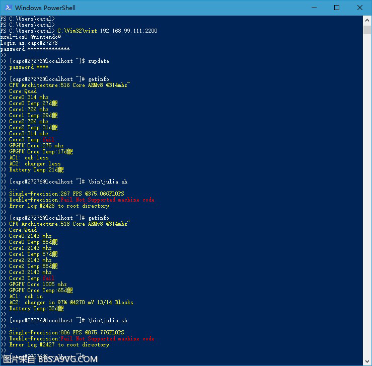
I don't think this is real (or, more accurately, I don't think it's a benchmark of the Switch hardware), but it's kind of interesting to try to figure out what it is.
There is a GPU benchmark named Julia (as it draws a Julia fractal) which runs on OpenGL and exists in both FP32 and FP64 versions (more details here), so it's likely that this is the benchmark being run. It reports results in FPS, although it doesn't report any measure of Gflops (there could be a separate simple FMA benchmark also included in the script for that, though).
The benchmark results, though, don't in any way match up to what Switch could do. The screenshot reports 806 fps in docked mode, however even a GTX 1070 only scores about 30% higher than that. In theory they could be running at a lower resolution (standard seems to be 1080p), but it would have to be a ludicrously low resolution for the results to make sense.
The Gflops reported are a little confusing. If it's a FMA (fused multiply-add) benchmark then you wouldn't expect numbers to quite hit the theoretical peak of the hardware, so I wouldn't necessarily expect nice round power-of-two results. It could also include both CPU and GPU benchmarks. However, it still doesn't really make any sense either from what we know of the Switch hardware, or from the reported Julia results. A 2 SM Maxwell/Pascal GPU at 1005MHz would have a theoretical maximum capability of 515 Gflops, and as far as I'm aware a quad-A57 at 2143MHz would have a theoretical maximum of 137 Gflops (although I'm open to correction on this). It simply wouldn't be possible for the two combined to hit 875 Gflops.
The Gflops also don't make sense when compared to the Julia benchmark results. To get 800fps in that test you'd expect a card somewhere in the 4-5Tflops range, not 875Gflops. Again I suppose you could run the test at 640x480 or something like that, but I can't imagine why someone would set up a benchmark to run at such a low resolution.
The high GFLOPS, the bash script and the mere 10C difference between standby and full-power do cause a serious doubt of the truthfulness of this screengrab. Also, I haven't seen an ARM cluster yet where cores can be individually clocked, but that could be a matter of performance governor after all.
The temp differences between idle and load actually make some degree of sense (CPU goes from ~29C to ~56C and GPU from 17C to 65C, it's the battery which only goes up from 21C to 32C). What confuses me is why the temperatures of the CPU and GPU are so different. If they're on the same die we'd expect only a couple of degrees difference, yet we're seeing 10+ degrees, which isn't something you'd see on an SoC. I suspect that the actual device they're testing (whatever it is) has a discrete GPU.
In theory the CPU cores could be split up into separate clusters, but it wouldn't seem to make much sense to do so for Switch, and if they were you would expect cores 0 & 1 and then cores 2 & 3 to be grouped together, not 0 grouped with 3 and 1 with 2.
Vampirolol
Member
Often these kind of people have amazing phones that can run PS4 Pro games like nothing else. For at least 9 hours.its always ugly. I know i'm not the most tech savy... but there is always a group that come on here and shout claims (mostly negative) and they have no idea what they are talking about.
What if they are 64 bit?
Then it would have to be 2 chips to hit 128bit, this is the reason why you buy 2 ram modules instead of 1. For the dual channel, as 1 chip is almost always cheaper, unless there is poor adoption, but we are talking the phone market, these high bandwidth chips will be in everything.
EdwardTivrusky
Member
I might sound like an idiot asking this but how exactly will people work out the full specs / clockspeeds etc of the chip when it releases and they can do teardowns? I find this stuff incredibly interesting but don't have the knowhow to do it myself.
They'll put oscilliscopes on the circuits for clock speeds etc, grind the tops off the chips to get scans of the innards, check serial numbers and look for specification/patent/design documents to get extra info and run some benchmarks to figure out performance.
Buggy Loop
Member
I don't think this is real (or, more accurately, I don't think it's a benchmark of the Switch hardware), but it's kind of interesting to try to figure out what it is.
There is a GPU benchmark named Julia (as it draws a Julia fractal) which runs on OpenGL and exists in both FP32 and FP64 versions (more details here), so it's likely that this is the benchmark being run. It reports results in FPS, although it doesn't report any measure of Gflops (there could be a separate simple FMA benchmark also included in the script for that, though).
The benchmark results, though, don't in any way match up to what Switch could do. The screenshot reports 806 fps in docked mode, however even a GTX 1070 only scores about 30% higher than that. In theory they could be running at a lower resolution (standard seems to be 1080p), but it would have to be a ludicrously low resolution for the results to make sense.
The Gflops reported are a little confusing. If it's a FMA (fused multiply-add) benchmark then you wouldn't expect numbers to quite hit the theoretical peak of the hardware, so I wouldn't necessarily expect nice round power-of-two results. It could also include both CPU and GPU benchmarks. However, it still doesn't really make any sense either from what we know of the Switch hardware, or from the reported Julia results. A 2 SM Maxwell/Pascal GPU at 1005MHz would have a theoretical maximum capability of 515 Gflops, and as far as I'm aware a quad-A57 at 2143MHz would have a theoretical maximum of 137 Gflops (although I'm open to correction on this). It simply wouldn't be possible for the two combined to hit 875 Gflops.
The Gflops also don't make sense when compared to the Julia benchmark results. To get 800fps in that test you'd expect a card somewhere in the 4-5Tflops range, not 875Gflops. Again I suppose you could run the test at 640x480 or something like that, but I can't imagine why someone would set up a benchmark to run at such a low resolution.
The temp differences between idle and load actually make some degree of sense (CPU goes from ~29C to ~56C and GPU from 17C to 65C, it's the battery which only goes up from 21C to 32C). What confuses me is why the temperatures of the CPU and GPU are so different. If they're on the same die we'd expect only a couple of degrees difference, yet we're seeing 10+ degrees, which isn't something you'd see on an SoC. I suspect that the actual device they're testing (whatever it is) has a discrete GPU.
In theory the CPU cores could be split up into separate clusters, but it wouldn't seem to make much sense to do so for Switch, and if they were you would expect cores 0 & 1 and then cores 2 & 3 to be grouped together, not 0 grouped with 3 and 1 with 2.
Just a quick update in case you missed it
It was translated by Dahuman that the benchmark was running @ 480x360
Just a quick update in case you missed it
It was translated by Dahuman that the benchmark was running @ 480x360
Thanks, I missed that, it makes more sense for the frame rates given. The Gflops given don't seem to bear any relation to Switch, though.
Just a quick update in case you missed it
It was translated by Dahuman that the benchmark was running @ 480x360
If thraktor can work out the flops problem, it could be a very early test of a different switch iteration.
Then it would have to be 2 chips to hit 128bit, this is the reason why you buy 2 ram modules instead of 1. For the dual channel, as 1 chip is almost always cheaper, unless there is poor adoption, but we are talking the phone market, these high bandwidth chips will be in everything.
Would be an interesting take on it. Wouldn't that be double the bus size of a normal Tegra X1? Could that be one of the chip customizations?
Would be an interesting take on it. Wouldn't that be double the bus size of a normal Tegra X1? Could that be one of the chip customizations?
Yeah, it would be easy enough to implement, it just depends on what the chip needs, I suspect a small on-die memory, like 4MB. Thraktor did some posts in another thread about Zelda's performance possibly be from hitting a tiling issue of post process effects, since stuff like dof can't be tiled.
Which is why I think the 64bit bus is fine for memory, the issue I have is 2 chips being an odd decision for final hardware but not matter much in a prototype of a limited run.
IE, 2 chips would suggest 128bit memory bus, though a July devkit would use 64bit.
Has there been any findings regarding the sd reader from the tear down, just trying to speculate and make a card purchase this week in prep of it arriving.
Well here's an image of it:

From the image we can see the code ODIN-uSD-X3, so presumably it has the power of the Norse god of war! Or, more likely, it's just a standard microSD reader with a normal max of ~95MB/s. Even in the very unlikely case that it is a UHS-II reader, UHS-II cards are still far more expensive than standard UHS-I cards, so I wouldn't really bother with them until prices come down.
LordOfChaos
Member
But 16nmFF ~ 20nm, almost same density. They fit 512 cores for GPU in there with 8 core CPU ArmV8 ? I mean yeah the chip is not ready, but size wise..
Those Tegra X1 on drive PX

vs Xavier

Really, i'm just trying to wrap my head around SoC similarities with 2x the # of cores. 16nmFF vs 20nm is not the sole explanation.
We need a banana for scale! Quick someone put the chips scaled vs Jen-Hsun Huang's head!
Again though, an IHS size != a chip size.
Look at Intel parts, plenty of them look the same from the IHS size when the chip inside is different, it's cheaper to stamp out the same IHS for everything.
If I read this right, this would mean a 64bit memory bus, right?
Yes, this is correct.
blu
Wants the largest console games publisher to avoid Nintendo's platforms.
Ah, I initially glossed over the grab and later mis-remembered it. Thank you for the correction.The temp differences between idle and load actually make some degree of sense (CPU goes from ~29C to ~56C and GPU from 17C to 65C, it's the battery which only goes up from 21C to 32C).
Well, it really depends on the size of the floorplan and the points they're monitoring. Approaching 10C of delta is achievable on the some dies, if they monitored t-junction at sufficiently remote locations. Now, whether they could load _all_ CPU cores, along with the GPU (and thus saturate the thermal map), and still get large differences is really up to the peculiarities of the specific floorplan. For instance, IIRC, I can get deltas of ~7C across certain cores on my Xeon without much issue, but that's at largely asymmetrical loads and at 22nm a xeon is not a small die.What confuses me is why the temperatures of the CPU and GPU are so different. If they're on the same die we'd expect only a couple of degrees difference, yet we're seeing 10+ degrees, which isn't something you'd see on an SoC. I suspect that the actual device they're testing (whatever it is) has a discrete GPU.
Right, clusterization can go in pairs as well, but it's traditionally done for binning purposes - when you have a SKU of 2 cores and a SKU of 4 cores, and you want to bin the smaller from the larger. I can't see such a use case for nintendo.In theory the CPU cores could be split up into separate clusters, but it wouldn't seem to make much sense to do so for Switch, and if they were you would expect cores 0 & 1 and then cores 2 & 3 to be grouped together, not 0 grouped with 3 and 1 with 2.
Again though, an IHS size != a chip size.
It's also unlikely that what he's holding is actually Xavier (given that the chip isn't due to even sample until late this year). Jen-Hsun Huang likes holding up chips, and it not being the right one hasn't stopped him before.
FunkyDealer
Banned
Well here's an image of it:
From the image we can see the code ODIN-uSD-X3, so presumably it has the power of the Norse god of war! Or, more likely, it's just a standard microSD reader with a normal max of ~95MB/s. Even in the very unlikely case that it is a UHS-II reader, UHS-II cards are still far more expensive than standard UHS-I cards, so I wouldn't really bother with them until prices come down.
Thor is the Norse god of war. Odin is the god of wisdom. So it's a wise choice by Nintendo.
blu
Wants the largest console games publisher to avoid Nintendo's platforms.
Heh, that's quite true.It's also unlikely that what he's holding is actually Xavier (given that the chip isn't due to even sample until late this year). Jen-Hsun Huang likes holding up chips, and it not being the right one hasn't stopped him before.
Well, one hypothetical scenario is they never upgraded the CCI to a newer one which would support HMP, so they could not physically run the OS on an A53 core while still doing a game on all the A57s.@Blu / @Thraktor
Any guesses as to why Nintendo might have chosen to (allegedly) remove A53s from the X1 and just let one core of the main CPU run the OS, as the leaked docs seem to imply?
Hmm thanks, I guess (due to almost zero knowledge on the specific subject) I was unintentionally making things easier than they actually are then. :-\Well, one hypothetical scenario is [...]
LordOfChaos
Member
That seems like a solid reason blu, I hadn't thought of that. Otherwise the 0.7mm2 Cortex A53s would have been trivial to keep in.
This may shed more light

Tegra X1 did not have the newer big.little revisions that would have allowed all core types to be used at once, it would have switched between the clusters. So that way you couldn't run the OS on a small core while running the game on the big core without updated the CCI as blu suggested.
Seems a shame to waste a big core on the OS, but it is what it is. Three A57 cores vs ~6.5 Jaguar cores would really make "switch CPU >>> PS4 CPU" a head scratcher.
Hmm thanks, I guess (due to almost zero knowledge on the specific subject) I was unintentionally making things easier than they actually are then. :-\
This may shed more light
Tegra X1 did not have the newer big.little revisions that would have allowed all core types to be used at once, it would have switched between the clusters. So that way you couldn't run the OS on a small core while running the game on the big core without updated the CCI as blu suggested.
Seems a shame to waste a big core on the OS, but it is what it is. Three A57 cores vs ~6.5 Jaguar cores would really make "switch CPU >>> PS4 CPU" a head scratcher.
That seems like a solid reason blu, I hadn't thought of that. Otherwise the 0.7mm2 Cortex A53s would have been trivial to keep in.
This may shed more light
Tegra X1 did not have the newer big.little revisions that would have allowed all core types to be used at once, it would have switched between the clusters. So that way you couldn't run the OS on a small core while running the game on the big core without updated the CCI as blu suggested.
Seems a shame to waste a big core on the OS, but it is what it is. Three A57 cores vs ~6.5 Jaguar cores would really make "switch CPU >>> PS4 CPU" a head scratcher.
It still doesn't make sense to remove them when they are so small and can run the OS, web browser, Netflix, vc games, etc. You'd just extend the battery life considerably. Instead they may never have browser just because it would kill the battery too fast. Of course browser is a security risk, but it is still interesting that they would remove it since it is trivial.
Skittzo0413
Member
That seems like a solid reason blu, I hadn't thought of that. Otherwise the 0.7mm2 Cortex A53s would have been trivial to keep in.
This may shed more light
Tegra X1 did not have the newer big.little revisions that would have allowed all core types to be used at once, it would have switched between the clusters. So that way you couldn't run the OS on a small core while running the game on the big core without updated the CCI as blu suggested.
Seems a shame to waste a big core on the OS, but it is what it is. Three A57 cores vs ~6.5 Jaguar cores would really make "switch CPU >>> PS4 CPU" a head scratcher.
I'm guessing 3x A72s would still be a bit behind the PS4 CPU too? Though maybe not at the Foxconn clocks. Either way that determination was likely made before core and clock numbers were final, as it's still stronger per core and per clock.
And as a reminder we still know nothing about the retail SoC besides the die size apparently.
EDIT: Here's a question as I'm on mobile and can't do the proper paint.net work- is there enough space below the two RAM modules to fit a differently sized RAM module as a replacement? As in, in the off chance that this is an old prototype or devkit, is it possible that the final RAM modules can be different (aka 64bit each) on the same motherboard?
I'm guessing 3x A72s would still be a bit behind the PS4 CPU too? Though maybe not at the Foxconn clocks. Either way that determination was likely made before core and clock numbers were final, as it's still stronger per core and per clock.
And as a reminder we still know nothing about the retail SoC besides the die size apparently.
3 A72 at those clocks would match the ps4 cpu in overall performance, likely still edging out the 6.5 cores for devs. Also single threaded performance is the biggest factor, and that chip would absolutely be far better for developers, offering much more power per thread and thus less busy work balancing cores for different tasks.
So I've been following this thread since the tear down and there's very little between the technical guesswork from knowledgeable folks and some sporadic "how many xbox's duct taped is it bros??"
Would a lovely gent be so kind as to roll up the current status of the data analysis into a basic "here's how it's looking" for us plain folk?
Would a lovely gent be so kind as to roll up the current status of the data analysis into a basic "here's how it's looking" for us plain folk?
So I've been following this thread since the tear down and there's very little between the technical guesswork from knowledgeable folks and some sporadic "how many xbox's duct taped is it bros??"
Would a lovely gent be so kind as to roll up the current status of the data analysis into a basic "here's how it's looking" for us plain folk?
Could be the July devkit configuration, could be final hardware. Could be 20nm, could be 16nm. RAM chips are about the only thing these details are good for except its potato footage and if it is July's configuration, we already know it and doesn't confirm final hardware. Basically it's a great look inside the device but it isn't speaking yet.
speaking of this I was just thinking... what ever happened to the CPU person on here? The one that stated and had all this history of being right on CPU performance. Didn't they say Switch was going to have the best CPU ahead of XB1. Is that dead now? Did they ever defended the reason or sources to why they made that statement?
They didn't think the cpu clock would be so low. We still aren't sure, but we could find A72 in the soc, that would be a pretty good sign eurogamer's clocks are no longer viable. We will know soon, so I'm just enjoying the speculation.
LordOfChaos
Member
3 A72 at those clocks would match the ps4 cpu in overall performance, likely still edging out the 6.5 cores for devs. Also single threaded performance is the biggest factor, and that chip would absolutely be far better for developers, offering much more power per thread and thus less busy work balancing cores for different tasks.
Seems a bit of a stretch. Single threaded A72 @ 1.4GHz posts 1400 here
https://browser.primatelabs.com/v4/cpu/1907257
Single threaded Jaguar @ 1.6Ghz posts 1100
https://browser.primatelabs.com/v4/cpu/1795638
Three @ 1.2GHz would make it hard to find a way to match up. At the "my uncle in China" foxconn 2GHz number we could get nearer.
lwilliams3
Member
speaking of this I was just thinking... what ever happened to the CPU person on here? The one that stated and had all this history of being right on CPU performance. Didn't they say Switch was going to have the best CPU ahead of XB1. Is that dead now? Did they ever defended the reason or sources to why they made that statement?
That was LCGeek. She stated after the Eurogamer story that they had the chipset correct, but she didn't know that they would clock them so low. Despite her constantly saying that it may be subject to change due to numerous factors even prior to that story, she got banned after the January 13th event.
Seems a bit of a stretch. Single threaded A72 @ 1.4GHz posts 1400 here
https://browser.primatelabs.com/v4/cpu/1907257
Single threaded Jaguar @ 1.6Ghz posts 1100
https://browser.primatelabs.com/v4/cpu/1795638
Three @ 1.2GHz would make it hard to find a way to match up. At the "my uncle in China" foxconn 2GHz number we could get nearer.
Actually, the foxconn number was something like 1.78GHz.. almost exactly 75% higher than the clockspeed from Eurogamer.
Seems a bit of a stretch. Single threaded A72 @ 1.4GHz posts 1400 here
https://browser.primatelabs.com/v4/cpu/1907257
Single threaded Jaguar @ 1.6Ghz posts 1100
https://browser.primatelabs.com/v4/cpu/1795638
You'd have to check more than a single benchmark, ps4's was posted in an old speculation thread against 4 A57 1ghz and found those cores about equal. Still 1.78ghz would give close to 1800 in that benchmark you have, while ps4's cpu would still post 1100. In this singular benchmark, the A72 core is 62% faster.
Buggy Loop
Member
With the photos of the board in this thread being so dated (FCC approval switch or early prototype)
There's so much right with Foxconn leaks so far that i don't think we can put that benchmark leak under the rugs..
I'm in team believe @ 512 cuda cores
thisisneogaf.gif
I don't care if it does not happen, i'm fine with just a TX1. But... "what if"..
There's so much right with Foxconn leaks so far that i don't think we can put that benchmark leak under the rugs..
I'm in team believe @ 512 cuda cores
thisisneogaf.gif
I don't care if it does not happen, i'm fine with just a TX1. But... "what if"..
Both the layout of all the passives on the package and the die size appear to be an exact match. That's not something I'd expect to just happen with radically different SoCs.What's indicated here? We literally just have a picture of the silicon and nothing else, and a bunch of people who are simply trying to match pictures of the back to indicate it's 1:1. It's ridiculous
There is no way in hell that the Switch will have UHS II support in speed even if it can access it, the pins are not the same. They would not shell out the money for it, at least not the first edition ones, maybe, and that's a big maybe, they will have it in later revisions or a Nintendo NEW(xN) Switch.Well here's an image of it:
From the image we can see the code ODIN-uSD-X3, so presumably it has the power of the Norse god of war! Or, more likely, it's just a standard microSD reader with a normal max of ~95MB/s. Even in the very unlikely case that it is a UHS-II reader, UHS-II cards are still far more expensive than standard UHS-I cards, so I wouldn't really bother with them until prices come down.
LordOfChaos
Member
You'd have to check more than a single benchmark, ps4's was posted in an old speculation thread against 4 A57 1ghz and found those cores about equal. Still 1.78ghz would give close to 1800 in that benchmark you have, while ps4's cpu would still post 1100. In this singular benchmark, the A72 core is 62% faster.
There's about 25 microbenchmarks listed within those. Whatever singular benchmark was posted before, I'd trust the culmination of all these more. Or look at a particular one of the 25 if it's more interesting.
1800 points at 1.78GHz would be relatively near 6.5 cores at 1100, but still decidedly under, not backing the statement "Switch CPU >>>> PS4 CPU", which is what I had been wondering at. That they're relatively close isn't what I'm arguing.
Of course the comment could have related to single threaded performance, where yes, the Switch would be ahead. Without any context whatsoever around the comment I guess it's not worth scratching my head over.
This is all speculation with the A72 anyways, that it's near exactly the TX1 die size to me strongly hints at 20nm and A57.
Keep expectations lowWith the photos of the board in this thread being so dated (FCC approval switch or early prototype)
There's so much right with Foxconn leaks so far that i don't think we can put that benchmark leak under the rugs..
I'm in team believe @ 512 cuda cores
thisisneogaf.gif
I don't care if it does not happen, i'm fine with just a TX1. But... "what if"..
It'd only make sense if they are talking about efficiency and not raw performance, I don't think people were under the delusion that the Switch CPU would run circles around what's in the APUs.There's about 25 microbenchmarks listed within those. Whatever singular benchmark was posted before, I'd trust the culmination of all these more.
1800 points at 1.78GHz would be relatively near 6.5 cores at 1100, but still decidedly under, not backing the statement "Switch CPU >>>> PS4 CPU", which is what I had been wondering at. That they're relatively close isn't what I'm arguing.
Similar threads
- 70
- 7K
Deerock71
replied
- Locked
- 12
- 2K