I was responding to someone saying that higher res like 1440P might not be accepted by the TV & I was saying why wouldn't the PS4 Neo be able to output the 1440P game at 1080P like PS4 does 1080P games at 720P & 480P. I'm not saying they should downscale a 1440P signal to 1080P on a 4K TV.
Why am I getting all these weird responses as if I'm suggesting that they downsample the games from a higher resolution?
I was responding to someone saying that 1440P might not be accepted by TVs & I was saying that it would work like when you have a 1080P game playing with the PS4 set to 480P or 720P.
i.e just set the PS4/Neo to a output that the TV will accept if it can't accept 1440P.
1080p TV, yes, downscale 1440p to it if you need to.
4K TV that would only accept a 1080p input for upscaling to 4K? Then you DO NOT want to downscale to 1080p on the PS4, as that would lose detail before it gets to the TV, you want to take the internal 1440P and upscale it PS4.5-side to the native 4K so that none of the pixel detail is lost.
Well of course both is always better, but you can't have both. A larger Zen CPU will either reduce available die size for the GPU meaning less CUs and lower power, or it'll produce a bigger, hotter, more expensive chip that might go beyond what Sony is willing to pay for.
Larger than what, exactly? Are four Zen cores larger than eight Jags? How much larger?
Sony has a history of going for GPU compute and I think PS4 backs that up. PS2 and PS3 were both heavily in that direction with the VUs and SPEs. PS4 with 'too much' GPU in the mix is IMO an extension of that philosophy. You have enough CPU to handle the household chores, and the rest is pushed onto the GPU.
Sure, but I don't think hobbling the CPU is the proper way to encourage more GPGPU use. Rather, I think it's better to continue encouraging it via the excellent hardware and software tools they have currently, and working to improve both. Eschewing a generational leap in CPU tech because you want people to get better with GPGPU sounds sorta like gouging out your eyes to help improve your hearing.
PCs happen to have powerful CPUs by default these days, so there you can do much more of the heavy lifting. And PC GPUs generally don't have good support for async compute. Add in the complexities of multiple configs and there is basically no incentive to use the GPU heavily on a PC title.
This creates a challenge for multiplatform developers of course. Providing a beefy CPU is a benefit for those devs that would like to bring a standard PC engine across.
Yeah, that's pretty much what I was saying; PC games are gonna need a reasonably strong CPU anyway because their engines can't rely on GPGPU as extensively, as much as we'd like them to. So even if gimping the CPU does somehow make exclusive devs better at GPGPU, it still sorta leaves the cross-platform guys with very little on their plates.
Plus, some stuff is just better to do on the CPU, and it's nice to be able to do lots of that stuff if you need or want to.
And 2 years after that, Scorpio 2 will leapfrog again. So it's totally up to AMD to make "true" jumps or not, in technical terms. Only determined by when Sony and MS release a new iteration of a console, not *who* does it.
To some extent, but they do have room to customize their designs to some extent. For example, Sony made a lot of enhancements to improve the performance of GPGPU stuff. We can use the roadmaps to get a basic idea of where everyone will be performance-wise barring any eSRAM-type blunders, obviously but that doesn't mean there's no longer room for surprises.
Well I was all on board, but than I realized how unlikely it would be for Sony to release a 5.5 TF machine with a 212 gb/s memory bandwidth. I love the speculation and believe everything OsirisBlack has said, but we haven't heard any new information regarding such a substantial spec change from any other sources outside Osiris. Until we do I'll stick with the conservative model.
This thread really has gone see-saw. The dev kits in current circulation does not indicate final hardware, it never has before. I don't know why people want to temper expectations on NEO hardware when the thing has not even been announced yet....
I just meant that nobody could ever be blown away by tech specs - like never again because consoles will never contain any "unknown" pieces of hardware again (or at least I don't think so but then again, FPGAs would be a good secret sauce of power ).
I think there is alot of misinterpretation happening here. Osiris never said Sony is going for the 5.5TF route. He said the following:
The first option with the power of the leaked specs (jaguar 2,1GHz) for 399$ is no longer considered by Sony.
Instead sony is undecided between two options:
1.Neo with a better CPU for 499$ (no word on more than 4.14 GPU power yet)
2.Neo with 5.5TF (no word on better CPU yet, but I would assume so) for 599$ or more
He says that Sony doesn't want to revisit the 599$ price point so the second option is very unlikely atm. They might go for a Q1 2017 release to get the price down to 499$ though.
What Osiris was told most recently by someone working at the mothership was that Sony didn't want to revisit $599, and they thought waiting until Q1 was the best way to hit the $499 price point, even if they go with Option B. Conversely, one assumes this means that launching holiday 2016 would make it difficult for them to hit $499, even if they go with Option A.
For clarity, going back to the original leak, Option A was effectively the same as the dev kits sent out 4.2TF and the 2.1GHz Jags. Option B would have a "better" CPU though no other CPU specifics, including architecture, were given and it was later clarified that Option B was always planned to have a 5.5TF GPU to go with its "better" CPU. We were also told these options were targeting $399 and $499 respectively, and they were tentatively targeting a Q1 2017 launch, whichever option they chose.
Then there was a lot of noise being made about Neo possibly launching 4Q16 rather than 1Q17, and Osiris said that "something happened," and suddenly Option A was now going to cost $499 rather than the $399 he was told back in March.
Which brings us back to the latest statement Sony wanna avoid $599, and think waiting until Q1 gives them the best chance to hit $499, even with Option B. So it sounds like launching this holiday means probably missing out on Option B, and potentially missing the $499 price point as well. My guess is that while AMD could potentially handle a Q4 launch, they won't be fully production-ready until later in Q1.
So again I ask, what's the rush? "Delaying" to their original plan of a Q1 launch still puts them out three quarters ahead of MS. It also leaves MS in the position of having nowhere to go but up, in a season when 99% of shoppers are looking for bargains.
Yields? 14nm/16nm is a new thing, and it takes a while to work out the kinks. The PS4's APU cost ~$100 to manufacture at launch. But that price basically just means they get an average of 150 useful chips from a $15,000 wafer of 161 chips. When a process is immature and yields are low, perhaps you have so many defects on every $15,000 wafer that you only get 75 useful APUs instead of 150. That means each one costs you an average of $200 to produce, boosting the price of your console by $100.
However, if you wait another six months for the chip makers to get more practice, then maybe you can start getting 150 useful chips per wafer, and you can launch at the $499 price point you were hoping to hit.
I assume you mean 5.5TF? Neither is 6TF, really. For example, to run something like Uncharted 4 exactly as it is right now same frame rate, AA, alpha effects, models, textures, etc., etc. and simply bump the resolution to 4k, you'd need a 7.36TF GPU, at least.
I've got no problems with anything I was just trying to point out that there was some epic miss-communication going on with folks :/ And then that turns in to more miss-communications of my own it seems where now Thruway thinks I'm telling everyone there is no secret sauce (I'm making zero claims about anything).
While I'm being honest here and with all due respect to the mods and Osiris I have quite a few issues with his info (I have asked questions) and how it comes across to me. Given nobody else seems to question any of the info and the mods are happy then I must be wrong.
That's the source I've been most focused on myself, but like I said earlier, I think Sony are releasing disinformation at this point. Hence, you need to use some common sense when trying to sort through conflicting information. My summary above makes the most sense to me, at least. lol
Think you've got that reversed. The (MUCH) larger percentage will be people replacing OG PS4's. Pretty much all of the early adopters that rocket console launches to multi-millions of units sold will buy a Neo. Holdouts buying their first PS4 now don't care about technology and are extremely price sensitive. They will buy a closeout price bomba OG PS4 over a Neo, or one of the deluge of used ones inevitably flooding CL/Ebay/Gamestop post Neo.
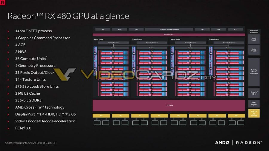
I have a feeling RX 480 and possibly Neo may become ROP-limited in many scenarios. It only still has 32 ROPs like the 7870 and PS4 GPU, but a massive 144 TMUs. Seems kinda unbalanced, even if it clocks up to 1.5GHz
End of the why low AF worries ? Also, TMU's are often how you load general data from memory for the compute shaders, so you end up relying on them for far more stuff than simply loading images.
That's 122mm2 at 14nm. The CPU looks to be about 1/3 so around 45mm2. That is almost 4x the size of the jaguar cores, and that's assuming you can use a 4c/8t CPU
I would be very surprised if European E3 for SCEE (Gamescom, PGW or other) not ended up being very similar to this past E3: updates on games like GT Sport or Wild and showing the remainder of those dozens of VR games that they talked about.
They invested a lot of money on VR (a mistake in my mind, because VR, at this point, and with hyperbole, is like paying 400 euros for a right analogue stick). They are going to market it heavily in the coming months.
I don't know much about chip making, but doesn't moving from 28nm to 14nm make your die features 1/4th scale?
I can't find specs for zen but it'll be much larger.
Here is a pic of a skylake CPU
That's 122mm2 at 14nm. The CPU looks to be about 1/3 so around 45mm2. That is almost 4x the size of the jaguar cores, and that's assuming you can use a 4c/8t CPU
Shouldn't we be looking at it from a perspective of what fits on our die? PS4's APU is 328mm2, so that seems like a reasonable target for Neo as well. So if we allot 45mm2 to four Zen cores, that leaves 283mm2 for the GPU. Can we fit ~40 CU in to that space at 14nm? CUs are quarter-scale as well, right?
Thats what I thought, but I *think* the finfet stuff takes up extra space. Seems you get a 1/2 scale.
Shouldn't we be looking at it from a perspective of what fits on our die? PS4's APU is 328mm2, so that seems like a reasonable target for Neo as well. So if we allot 45mm2 to four Zen cores, that leaves 283mm2 for the GPU. Can we fit ~40 CU in to that space at 14nm? CUs are quarter-scale as well, right?
Oh? I thought a 4mm row of transistors became 2mm long, so quarter-scale on a plane. What even is finfet? What's so good about it if it's taking up half of your die space?
14nm is still starting out. GTX 1080 is only a 300mm2. A 320mm2 14nm APU would (1) be an absolute beast, and (2) crazily expensive.
Expensive enough that Sony may need to hold off until Q1 to hit $499?
But yeah, I was actually thinking the new die would be smaller overall even with double the CU count thanks 1/4-scale features, but I'm guessing the CUs are also 1/2-scale because finfet? Got any more info on this, because it sounds pretty poopy. lol
"that VR crap" is Sony's big release this year. It would be difficult for them to market and sell two new pieces of hardware at around the same time, and get the messaging around them just right without it looking like you need a neo for VR (Because I'm sure they'll want to point out how good neo will be for VR).
They need to give PSVR enough space to be its own thing, and for people to be comfortable that it is designed to work well with the PS4. Then launch neo, also as its own thing with the benefits it brings.
Oh? I thought a 4mm row of transistors became 2mm long, so quarter-scale on a plane. What even is finfet? What's so good about it if it's taking up half of your die space?
Expensive enough that Sony may need to hold off until Q1 to hit $499?
But yeah, I was actually thinking the new die would be smaller overall even with double the CU count thanks 1/4-scale features, but I'm guessing the CUs are also 1/2-scale because finfet? Got any more info on this, because it sounds pretty poopy. lol
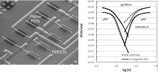
not entirely sure about finfet but it is a technology they introduced to help them get down to the smaller processes and chips. I guess it is there to reduce current leakage etc. So you don't get the full benefits of a simple 28-14nm shrink.
When they go down to 10/7nm (if), you might get the proper benefits there if they continue to use finfet, becuase that has already been factored into the current chips.
Yeah, I did a little reading too, and it seems the "28nm" or whatever refers to the length of some feature on the transistor, and because FinFET is a new way of building transistors, while that particular feature is indeed half the length it was in planar transistors, the "performance per square mm" isn't quite as high.
Oh, I also learned Intel's transistors are totally different than everyone else's — tri-gate versus dual-gate — so those Skylake cores may not necessarily be representative of Zen cores, size-wise. I guess we may not know how big Zen cores are until they start showing them.
Out of curiosity, how long had 28nm stuff been around when PS4 launched? Just wondering about the relative maturity of the two processes.
Yeah, I did a little reading too, and it seems the "28nm" or whatever refers to the length of some feature on the transistor, and because FinFET is a new way of building transistors, while that particular feature is indeed half the length it was in planar transistors, the "performance per square mm" isn't quite as high.
Oh, I also learned Intel's transistors are totally different than everyone else's tri-gate versus dual-gate so those Skylake cores may not necessarily be representative of Zen cores, size-wise. I guess we may not know how big Zen cores are until they start showing them.
Out of curiosity, how long had 28nm stuff been around when PS4 launched? Just wondering about the relative maturity of the two processes.
for GPUs it looks like the 7970 from AMD was the first, at the end of 2011/start of 2012. So about 2 years before PS4 launch, maybe 18 months before start of PS4 production?
for GPUs it looks like the 7970 from AMD was the first, at the end of 2011/start of 2012. So about 2 years before PS4 launch, maybe 18 months before start of PS4 production?
From my reading, as you reduce the node size you decrease forward current (ON or high state 1) which makes the transistor more efficient but leakage current (OFF Low state 0) increases. FinFET reduces leakage current when in the LOW state. The PS4 FinFET being used for NEO would be the second higher power version.
Efficiency increases lower the TDP which allows for increasing transistor count and density. Density reduces trace length and allows for lower drive current and voltage which increases efficiency.
The 2015 AMD PS4 APU @ 28nm on Global Foundries process had a higher density so it used less power compared to the launch PS4 APU.
My understanding is the NEO design is limited by TDP and a balance between GPU and CPU power use is made. A more powerful CPU using more power means a GPU that has to be clocked lower to keep the same TDP. For a Polaris dGPU design @ 150 watts that does 5.5TF would be reduced slightly with Jaguar mobile low power CPUs to about 5TF while using eExcavator or ZEN would reduce the GPU to about 4 TF. All this speculation on NEO TF appears to be backwards.
Hardware. Any higher clocking would have to be done within the threshold of the rest of the box. If you clock too high, you'll run into overheating issues and RROD-esque problems.
Hardware. Any higher clocking would have to be done within the threshold of the rest of the box. If you clock too high, you'll run into overheating issues and RROD-esque problems.
for GPUs it looks like the 7970 from AMD was the first, at the end of 2011/start of 2012. So about 2 years before PS4 launch, maybe 18 months before start of PS4 production?
Thinking about this a bit more, if we really are that close to the birth of this node, then yes, the difference between early-Q4 and late-Q1 may be pretty significant in terms of yields/costs, performance, new architectures being ready, etc.
From my reading, as you reduce the node size you decrease forward current (ON or high state 1) which makes the transistor more efficient but leakage current (OFF Low state 0) increases. FinFET reduces leakage current when in the LOW state. The PS4 FinFET being used for NEO would be the second higher power version.
Efficiency increases lower the TDP which allows for increasing transistor count and density. Density reduces trace length and allows for lower drive current and voltage which increases efficiency.
The 2015 AMD PS4 APU @ 28nm on Global Foundries process had a higher density so it used less power compared to the launch PS4 APU.
My understanding is the NEO design is limited by TDP and a balance between GPU and CPU power use is made. A more powerful CPU using more power means a GPU that has to be clocked lower to keep the same TDP. For a Polaris dGPU design @ 150 watts that does 5.5TF would be reduced slightly with Jaguar mobile low power CPUs to about 5TF while using eExcavator or ZEN would reduce the GPU to about 4 TF. All this speculation on NEO TF appears to be backwards.
Per Wikipedia, a 4-core Zen shouldn't pull any more than 35W. RX480 pulls ~113W at 5.8TF. Sounds like both should fit nicely in to a 150W APU, unless I'm missing something? Also, I'm not sure whether the 150W budget for PS4 includes the memory, but the TDP figure for the RX480 does, I believe.
I read HBM2 production is "getting in to full swing." If Neo launches ~GDC with HBM2, how will that affect its power budget?
Oh? I thought a 4mm row of transistors became 2mm long, so quarter-scale on a plane. What even is finfet? What's so good about it if it's taking up half of your die space?
Thinking about this a bit more, if we really are that close to the birth of this node, then yes, the difference between early-Q4 and late-Q1 may be pretty significant in terms of yields/costs, performance, new architectures being ready, etc.
Per Wikipedia, a 4-core Zen shouldn't pull any more than 35W. RX480 pulls ~113W at 5.8TF. Sounds like both should fit nicely in to a 150W APU, unless I'm missing something? Also, I'm not sure whether the 150W budget for PS4 includes the memory, but the TDP figure for the RX480 does, I believe.
I read HBM2 production is "getting in to full swing." If Neo launches ~GDC with HBM2, how will that affect its power budget?
150W is what I expect Neo to aim for at the wall i.e. around the the same as OG PS4. You are also forgetting a lot of stuff that comes within that 150W. HDD, Blu Ray drive, secondary chip+RAM, WiFi+Bluetooth etc then factor in PSU losses...
serversurfer said:
I assume you mean 5.5TF? Neither is 6TF, really. For example, to run something like Uncharted 4 exactly as it is right now — same frame rate, AA, alpha effects, models, textures, etc., etc. — and simply bump the resolution to 4k, you'd need a 7.36TF GPU, at least.
On the flipside, we have heard from some developers that the 8GB of memory found in PlayStation Neo isn't quite enough to get the most out of 4K displays.
If that is true, it would be pointless going higher than 4.2 TF anyway if the RAM isn't there to make use of more power? Just to make things clear DF actually mean 5.5GB because that is what is available for games.
I assume you mean 5.5TF? Neither is 6TF, really. For example, to run something like Uncharted 4 exactly as it is right now same frame rate, AA, alpha effects, models, textures, etc., etc. and simply bump the resolution to 4k, you'd need a 7.36TF GPU, at least.
Not just FLOPS or shaders - depending on clocks you'd need to have more or less quadruple the ROPS, TMUs and memory bandwidth as the current GPU. Maybe double the L2 cache or more as well
You mean Bonaire was based in PS4's GPU because Pitcairn is GCN 1.1 while PS4 is GCN 1.2 where late it give birth to Bonaire (AMD used Sony changes to create GCN 1.2).
150W is what I expect Neo to aim for at the wall i.e. around the the same as OG PS4. You are also forgetting a lot of stuff that comes within that 150W. HDD, Blu Ray drive, secondary chip+RAM, WiFi+Bluetooth etc then factor in PSU losses...
Well, the PS4 has a 250W supply. I assumed the 150W Jeff referenced was for the APU and possibly the main RAM too, and all that other stuff ran on the remaining 100W. Is that not the case? Regardless, apparently the main reason the PS4 "only" has a 250W supply was so they could use a two-prong power cord. The PS3 has a 380W (internal) supply, so Sony could go hotter than 250W if they needed to, but it sounds like 150W should give them enough elbow room anyway.
If that is true, it would be pointless going higher than 4.2 TF anyway if the RAM isn't there to make use of more power? Just to make things clear DF actually mean 5.5GB because that is what is available for games.
Oh, I see. Then yeah, that too. lol Sure, increasing the resolution means increasing the size of the frame buffer, if nothing else. Plus, you'll probably wanna have higher-res textures too, which means still more RAM.
Not just FLOPS or shaders - depending on clocks you'd need to have more or less quadruple the ROPS, TMUs and memory bandwidth as the current GPU. Maybe double the L2 cache or more as well
Well, yeah, I figured it was assumed that the GPU would have all of the additional hardware necessary to support whatever speed it was capable of. But the real point is that neither platform is likely to get a large enough performance bump to make 4k feasible; Scorpio would need to be at least 25% faster than announced. I think 4k would be kind of a waste of power even if the new boxen were gonna be 7.5TF+. I'd say it's probably better to stick with 1080p and double the frame rates to satisfy any performance wonks, then spend whatever's left on candy.
Each HWS does the work of a pair of ACEs and then some. Each HWS manages 16 queues, giving it a little more scheduling flexibility than an ACE which can only see and manage 8 queues. All their cards are set up like that now.
You mean Bonaire was based in PS4's GPU because Pitcairn is GCN 1.1 while PS4 is GCN 1.2 where late it give birth to Bonaire (AMD used Sony changes to create GCN 1.2).
Wrong, Pitcairn is the first GCN (1.0), Bonaire is 1.1 and used for the Xbox One's GPU.
PS4 is indeed GCN 1.0, it's basically a 7870 with 2 CUs disabled for yield.
Wrong, Pitcairn is the first GCN (1.0), Bonaire is 1.1 and used for the Xbox One's GPU.
PS4 is indeed GCN 1.0, it's basically a 7870 with 2 CUs disabled for yield.
PS4 has most/all of the features that ended up in GCN 1.2, like 8 ACEs for example. Many of those features were suggested by Sony and offered to AMD for free to roll back in to GCN, on the condition that none of Sony's contributions made it in to the Bone.
Sony collaborated similarly with IBM on Cell, except IBM turned around and put a lot of Sony's ideas in to the 360. Hence the new clause in their agreement with AMD.
I hope not. I am hoping for a November release, this gives the PSVR it's own launch time frame and spot light. I really hope it does come out this year, I want something new and shinny for the holidays and a PS4K (I think this will be the name) would fit the bill nicely.
Didn't they update the Aces to do more jobs? if that's the case it could still be used for PS4 Neo because each new Ace could be equaled to 2 or 4 old Aces
Well, the PS4 has a 250W supply. I assumed the 150W Jeff referenced was for the APU and possibly the main RAM too, and all that other stuff ran on the remaining 100W. Is that not the case? Regardless, apparently the main reason the PS4 "only" has a 250W supply was so they could use a two-prong power cord. The PS3 has a 380W (internal) supply, so Sony could go hotter than 250W if they needed to, but it sounds like 150W should give them enough elbow room anyway.
I think you are confusing the PSU rating with actual consumption. I think the main reason PS3 and PS4 have a 380W and 250W PSU is that they are most efficient at 40-60% load.
While playing games the PS3 at launch used a max of ~210W at the wall and PS4 a max of ~150w. Right in the sweet spot of the PSU rating.
Was it the Scorpio spec analysis article that DF mentioned they had info on how Neo plans to upscale and that it was interesting? Any update from them on that?
That is essentially all the active parts of components that go into an IC. The metal layers in a typical digital IC are for interconnects. You can make smaller transistors, but you then have to take care that the metal interconnects aren't patterned in such a way that it requires 16/14nm precision, i.e. avoiding contact from two separate traces.
Wrong, Pitcairn is the first GCN (1.0), Bonaire is 1.1 and used for the Xbox One's GPU.
PS4 is indeed GCN 1.0, it's basically a 7870 with 2 CUs disabled for yield.
Both consoles are based on GCN Gen 2 IP-Blocks (1.1) and there is no Pitcairn/Bonaire in there, although many like to make the comparison, because these dGPUs are configured nearly indentical, it's wrong in detail.
All console chips are unique designs.
")